- 您現(xiàn)在的位置:買賣IC網(wǎng) > PDF目錄385765 > R2023T (Ricoh Co., Ltd.) 2-wire Serial Interface Real Time Clock IC PDF資料下載
參數(shù)資料
| 型號: | R2023T |
| 廠商: | Ricoh Co., Ltd. |
| 英文描述: | 2-wire Serial Interface Real Time Clock IC |
| 中文描述: | 2線串行接口實(shí)時(shí)時(shí)鐘芯片 |
| 文件頁數(shù): | 14/50頁 |
| 文件大?。?/td> | 512K |
| 代理商: | R2023T |
第1頁第2頁第3頁第4頁第5頁第6頁第7頁第8頁第9頁第10頁第11頁第12頁第13頁當(dāng)前第14頁第15頁第16頁第17頁第18頁第19頁第20頁第21頁第22頁第23頁第24頁第25頁第26頁第27頁第28頁第29頁第30頁第31頁第32頁第33頁第34頁第35頁第36頁第37頁第38頁第39頁第40頁第41頁第42頁第43頁第44頁第45頁第46頁第47頁第48頁第49頁第50頁

R2023K/T
*1), *2) When the oscillation adjustment circuit is used, the interrupt cycle will fluctuate once per 20sec. or
60sec. as follows:
Pulse Mode: The “L” period of output pulses will increment or decrement by a maximum of
±
3.784 ms. For
example, 1-Hz clock pulses will have a duty cycle of 50
±
0.3784%.
Level Mode: A periodic interrupt cycle of 1 second will increment or decrement by a maximum of
±
3.784 ms.
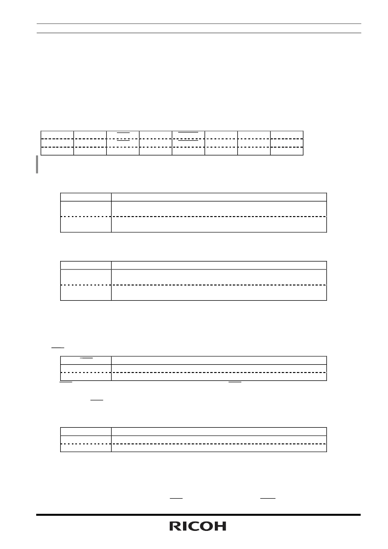
Control Register 2 (Address Fh)
D7
D6
D5
D4
D3
VDSL
VDET
XST
PON
CLEN1
VDSL
VDET
XST
PON
CLEN1
0
0
Indefinite
1
0
*) Default settings: Default value means read / written values when the PON bit is set to “1” due to VDD
power-on from 0 volts.
(1) VDSL
VDD Supply Voltage Monitoring Threshold Selection Bit
VDSL
0
Selecting the VDD supply voltage monitoring threshold setting of
1.6v.
1
Selecting the VDD supply voltage monitoring threshold setting of
1.3v.
The VDSL bit is intended to select the VDD supply voltage monitoring threshold settings.
(2) VDET
Supply Voltage Monitoring Result Indication Bit
VDET
0
Indicating supply voltage above the supply voltage monitoring
threshold settings.
1
Indicating supply voltage below the supply voltage monitoring
threshold settings.
Once the VDET bit is set to 1, the supply voltage monitoring circuit will be disabled while the VDET bit will
hold
the setting of 1. The VDET bit accepts only the writing of 0, which restarts the supply voltage monitoring
circuit. Conversely, setting the VDET bit to 1 causes no event.
(3)
XST
Oscillation Halt Sensing Monitor Bit
XST
0
Sensing a halt of oscillation
1
Sensing a normal condition of oscillation
The
XST
accepts the reading and writing of 0 and 1. The
XST
bit will be set to 0 when the oscillation
halt
sensing. The
XST
bit will hold 0 even after the restart of oscillation.
(4) PON
Power-on-reset Flag Bit
PON
0
Normal condition
1
Detecting VDD power-on -reset
The PON bit is for sensing power-on reset condition.
* The PON bit will be set to 1 when VDD power-on from 0 volts. The PON bit will hold the setting of 1 even
after power-on.
* When the PON bit is set to 1, all bits will be reset to 0, in the Oscillation Adjustment Register, Control
Register 1, and Control Register 2, except
XST
and PON. As a result, INTR pin stops outputting.
* The PON bit accepts only the writing of 0. Conversely, setting the PON bit to 1 causes no event.
14
D2
CTFG
CTFG
0
D1
D0
DAFG
DAFG
0
WAFG
WAFG
0
(For Writing)
(For Reading)
Default Settings *)
Description
(Default)
Description
(Default)
Description
Description
(Default)
相關(guān)PDF資料 |
PDF描述 |
|---|---|
| R2023T-E2 | 2-wire Serial Interface Real Time Clock IC |
| R2025D | High precision I2C-Bus Real-Time Clock Module |
| R2025S | High precision I2C-Bus Real-Time Clock Module |
| R5326Z003B | Automatic Mode Shift 2ch 150mA LDO |
| R5326Z004A | Automatic Mode Shift 2ch 150mA LDO |
相關(guān)代理商/技術(shù)參數(shù) |
參數(shù)描述 |
|---|---|
| R2023T-E2 | 制造商:RICOH 制造商全稱:RICOH electronics devices division 功能描述:2-wire Serial Interface Real Time Clock IC |
| R2-0257-02 | 制造商:Southco 功能描述: |
| R2-0259-02 | 制造商:Southco 功能描述: |
| R2025D | 制造商:RICOH 制造商全稱:RICOH electronics devices division 功能描述:High precision I2C-Bus Real-Time Clock Module |
| R2025S | 制造商:RICOH 制造商全稱:RICOH electronics devices division 功能描述:High precision I2C-Bus Real-Time Clock Module |
發(fā)布緊急采購,3分鐘左右您將得到回復(fù)。