- 您現(xiàn)在的位置:買賣IC網(wǎng) > PDF目錄382381 > PCF2105MU (NXP Semiconductors N.V.) LCD controller/driver PDF資料下載
參數(shù)資料
| 型號: | PCF2105MU |
| 廠商: | NXP Semiconductors N.V. |
| 英文描述: | LCD controller/driver |
| 中文描述: | LCD控制器/驅(qū)動器 |
| 文件頁數(shù): | 16/48頁 |
| 文件大?。?/td> | 289K |
| 代理商: | PCF2105MU |
第1頁第2頁第3頁第4頁第5頁第6頁第7頁第8頁第9頁第10頁第11頁第12頁第13頁第14頁第15頁當(dāng)前第16頁第17頁第18頁第19頁第20頁第21頁第22頁第23頁第24頁第25頁第26頁第27頁第28頁第29頁第30頁第31頁第32頁第33頁第34頁第35頁第36頁第37頁第38頁第39頁第40頁第41頁第42頁第43頁第44頁第45頁第46頁第47頁第48頁

1998 Jul 30
16
Philips Semiconductors
Product specification
LCD controller/driver
PCF2105
8.15
Programming of the MUX rate 1 : 32
With the MUX rate 1 : 32 the PCF2105 can be used in the
following ways:
To drive a 2-line display of 24 characters, use instruction
‘function set’ to set bit M to logic 0 and bit N to logic 1
To drive a 4-line display of 12 characters, use instruction
‘function set’ to set both bits M and N to logic 1.
8.16
Reset function
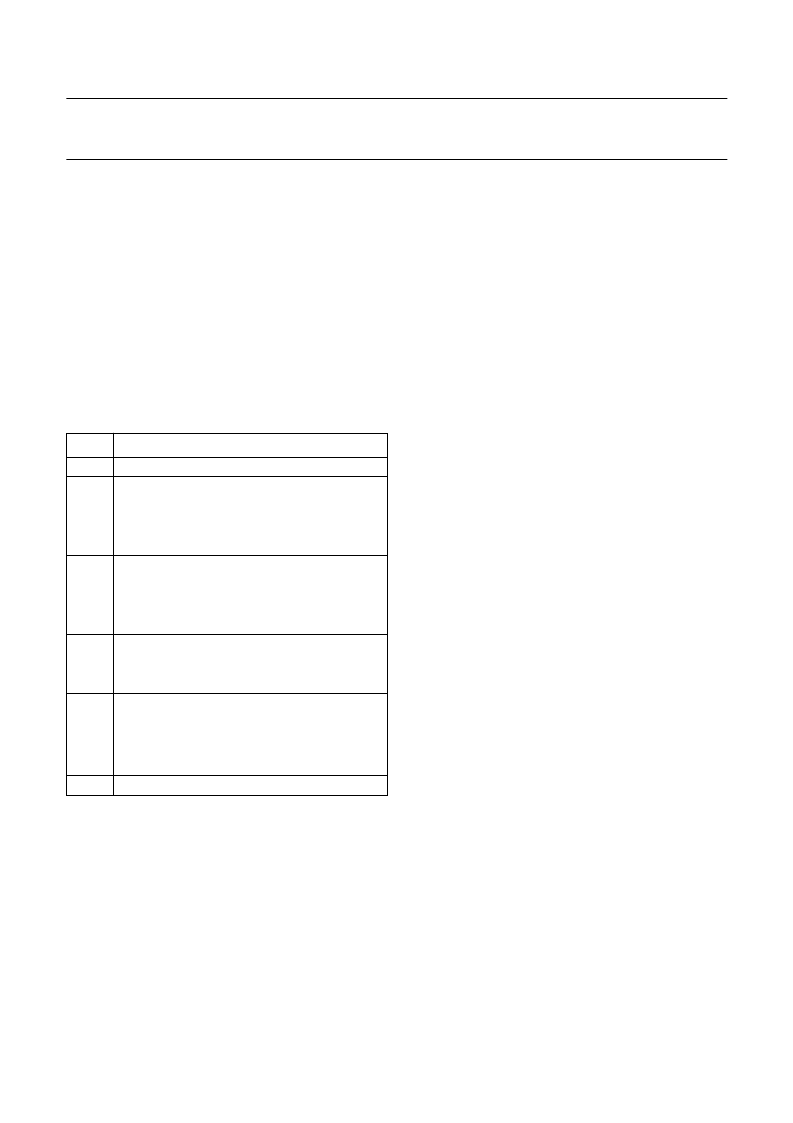
The PCF2105 automatically initializes (resets) when
power is turned on. The state after reset is given in Table 2
(see Tables 3 and 4 for the description of the bits).
Table 2
State after reset
9
INSTRUCTIONS
Only two PCF2105 registers, the Instruction Register (IR)
and the Data Register (DR) can be directly controlled by
the microcontroller. Before internal operation, control
information is stored temporarily in these registers to allow
interface to various types of microcontrollers which
operate at different speeds or to allow interfacing to
peripheral control ICs. The PCF2105 operation is
controlled by the instructions shown in Table 3 together
with their execution time. Details are explained in
subsequent sections.
STEP
DESCRIPTION
1
2
clear display
function set:
bit DL = 1: 8-bit interface
bits M and N = 0: 1-line display
bit G = 0: not used
display control:
bit D = 0: display off
bit C = 0: cursor off
bit B = 0: blink off
entry mode set:
bit I/D = 1: +1(increment)
bit G = 0: not used
default address pointer to DDRAM; the busy
flag indicates the busy state (BF = 1) until
initialization ends; the busy state lasts 2 ms;
the chip may also be initialized by software;
see Tables 10 and 11.
I
2
C-bus interface reset
3
4
5
6
Instructions are of 4 categories, those that:
1.
Designate PCF2105 functions such as display format,
data length, etc.
2.
Set internal RAM addresses
3.
Perform data transfer with internal RAM
4.
Others.
In normal use, category 3 instructions are used most
frequently. However, automatic incrementing by 1 (or
decrementing by 1) of internal RAM addresses after each
data write lessens the microcontroller program load.
The display shift in particular can be performed
concurrently with display data write, thus enabling the
designer to develop systems in minimum time with
maximum programming efficiency.
During internal operation, no instruction other than the
‘read busy flag and address’ will be executed.
Because the busy flag is set to logic 1 while an instruction
is being executed, it is advisable to ensure that the flag is
set to logic 0 before sending the next instruction or wait for
the maximum instruction execution time, as given in
Table 3. An instruction sent while the busy flag is HIGH will
not be executed.
9.1
Clear display
‘Clear display’ writes space code 20 (hexadecimal) into all
DDRAM addresses (the character pattern for character
code 20 must be a blank pattern), sets the DDRAM
address counter to logic 0 and returns the display to its
original position if it was shifted. Consequently, the display
disappears and the cursor or blink position goes to the left
edge of the display (the first line if 2 or 4 lines are
displayed) and sets bit I/D of ‘entry mode set’ to logic 1
(increment mode). Bit S of ‘entry mode set’ does not
change.
The instruction ‘clear display’ requires extra execution
time. This may be allowed for checking the Busy Flag (BF)
or by waiting until 2 ms has elapsed. The latter must be
applied where no read-back options are available, as in
some Chip-On-Glass (COG) applications.
9.2
Return home
‘Return home’ sets the DDRAM address counter to logic 0
and returns the display to its original position if it was
shifted. DDRAM contents do not change. The cursor or
blink position goes to the left of the display (the first line if
2 or 4 lines are displayed). Bits I/D and S of ‘entry mode
set’ do not change.
相關(guān)PDF資料 |
PDF描述 |
|---|---|
| PCF26100 | Bluetooth Adapter IC |
| PCF26100ET | DVI_D - DVI_D SINGLE LINK CABLE 5M BLK RoHS Compliant: Yes |
| PCF3F10B | Analog IC |
| PCF3F160 | Analog IC |
| PCF3F30 | Analog IC |
相關(guān)代理商/技術(shù)參數(shù) |
參數(shù)描述 |
|---|---|
| PCF2105MU/2 | 制造商:PHILIPS 制造商全稱:NXP Semiconductors 功能描述:LCD controller/driver |
| PCF2105MU/7 | 制造商:未知廠家 制造商全稱:未知廠家 功能描述:LCD Display Driver |
| PCF210AA | 制造商:PHILIPS 制造商全稱:NXP Semiconductors 功能描述:SPI Real time clock/calendar Time keeping application |
| PCF2110 | 制造商:未知廠家 制造商全稱:未知廠家 功能描述:LCD Display Driver |
| PCF2111 | 制造商:PHILIPS 制造商全稱:NXP Semiconductors 功能描述:LCD drivers |
發(fā)布緊急采購,3分鐘左右您將得到回復(fù)。