- 您現(xiàn)在的位置:買賣IC網(wǎng) > PDF目錄382380 > PCD5003H (NXP SEMICONDUCTORS) Advanced POCSAG Paging Decoder PDF資料下載
參數(shù)資料
| 型號: | PCD5003H |
| 廠商: | NXP SEMICONDUCTORS |
| 元件分類: | 尋呼電路 |
| 英文描述: | Advanced POCSAG Paging Decoder |
| 中文描述: | TELECOM, PAGING DECODER, PQFP32 |
| 封裝: | 7 X 7 MM, 1.40 MM HEIGHT, PLASTIC, SOT-358-1, LQFP-32 |
| 文件頁數(shù): | 28/44頁 |
| 文件大?。?/td> | 187K |
| 代理商: | PCD5003H |
第1頁第2頁第3頁第4頁第5頁第6頁第7頁第8頁第9頁第10頁第11頁第12頁第13頁第14頁第15頁第16頁第17頁第18頁第19頁第20頁第21頁第22頁第23頁第24頁第25頁第26頁第27頁當前第28頁第29頁第30頁第31頁第32頁第33頁第34頁第35頁第36頁第37頁第38頁第39頁第40頁第41頁第42頁第43頁第44頁

1997 Jun 24
28
Philips Semiconductors
Product specification
Advanced POCSAG Paging Decoder
PCD5003
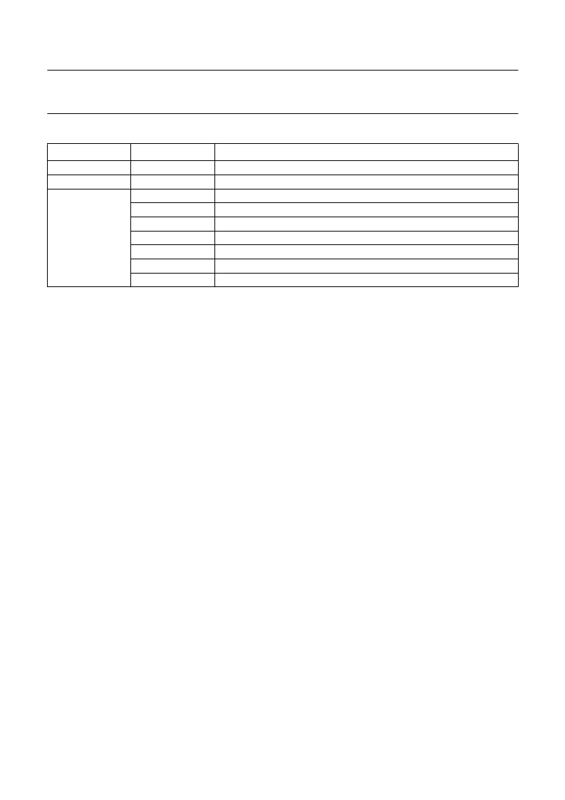
Table 27
Identifier bit allocation
Notes
1.
The bit numbering corresponds with the numbering in a POCSAG codeword: bit 1 is the flag bit
(0 = address, 1 = message).
A UPSW needs 18 bits to be matched for successful identification. Bit 1 (MSB) must be logic 0; bits 2 to 19 contain
the identifier bit pattern; they are followed by 2 predetermined random (function) bits and the UPSW is completed by
10 CRC error correction bits and an even-parity bit.
Bits FR3 to FR1 (MSB: FR3) contain the 3 least significant bits of the 21-bit RIC.
Identifiers 1 and 2 (RIC only) will be disabled by programming bit D2 as logic 0.
2.
3.
4.
BYTE
BIT (MSB: D7)
DESCRIPTION
1
2
D7 to D0
D7 to D0
D7 and D6
D5
D4
D3
D2
D1
D0
bits 2 to 9 of POCSAG codeword (RIC or UPSW); notes 1 and 2
bits 10 to 17
bits 18 and 19
frame number bit FR3 (RIC); note 3
frame number bit FR2 (RIC)
frame number bit FR1 (RIC)
identifier type selection (0 = UPSW, 1 = RIC); note 4
identifier enable (1 = enabled)
reserved for future use, logic 0 when read
3
7.57
Voltage doubler
An on-chip voltage doubler provides an unregulated DC
output for supplying an LCD or a low power microcontroller
on output V
PO
. An external ceramic capacitor of typical
100 nF is required between pins CCN and CCP. The
voltage doubler is enabled via SPF programming.
7.58
Level-shifted interface
All interface lines are suited for communication with a
microcontroller operating from a higher supply voltage.
The external device must have a common reference at V
SS
of the PCD5003.
The reference voltage for the level-shifted interface must
be applied to input V
PR
. This could be the on-chip voltage
doubler output V
PO
if required. When the microcontroller
has a separate (regulated) supply this separate supply
voltage should be connected to V
PR
.
The level-shifted interface lines are: RST, DON, ALC,
REF, INT.
The I
2
C-bus interface lines SDA and SCL can be
level-shifted independently of V
PR
by means of the
standard external pull-up resistors.
7.59
Signal test mode
A special ‘signal test’ mode is available for monitoring the
performance of a receiver circuit together with the
front-end of the PCD5003.
For this purpose the output of the digital noise filter and the
recovered bit clock are made available at outputs REF and
INT respectively. All synchronization and decoding
functions are normally active.
The ‘signal test’ mode is activated/deactivated by SPF
programming.
相關(guān)PDF資料 |
PDF描述 |
|---|---|
| PCD5008 | FLEX Pager Decoder |
| PCD5008H | FLEX Pager Decoder |
| PCD5013 | FLEX roaming decoder II |
| PCD5013H | FLEX roaming decoder II |
| PCD5032 | ADPCM CODEC for digital cordless telephones |
相關(guān)代理商/技術(shù)參數(shù) |
參數(shù)描述 |
|---|---|
| PCD5003HB-T | 制造商:未知廠家 制造商全稱:未知廠家 功能描述:Telecommunication Decoder |
| PCD5003U/10 | 制造商:PHILIPS 制造商全稱:NXP Semiconductors 功能描述:Advanced POCSAG Paging Decoder |
| PCD5008 | 制造商:PHILIPS 制造商全稱:NXP Semiconductors 功能描述:FLEX Pager Decoder |
| PCD5008H | 制造商:PHILIPS 制造商全稱:NXP Semiconductors 功能描述:FLEX Pager Decoder |
| PCD5008HBD-T | 制造商:未知廠家 制造商全稱:未知廠家 功能描述:Telecommunication Decoder |
發(fā)布緊急采購,3分鐘左右您將得到回復。