- 您現(xiàn)在的位置:買賣IC網 > PDF目錄299581 > ORLI10G-1BM680 FPGA, 1296 CLBS, 380000 GATES, PBGA680 PDF資料下載
參數(shù)資料
| 型號: | ORLI10G-1BM680 |
| 元件分類: | FPGA |
| 英文描述: | FPGA, 1296 CLBS, 380000 GATES, PBGA680 |
| 封裝: | PLASTIC, MULTILAYER, BGA-680 |
| 文件頁數(shù): | 30/74頁 |
| 文件大?。?/td> | 1411K |
| 代理商: | ORLI10G-1BM680 |
第1頁第2頁第3頁第4頁第5頁第6頁第7頁第8頁第9頁第10頁第11頁第12頁第13頁第14頁第15頁第16頁第17頁第18頁第19頁第20頁第21頁第22頁第23頁第24頁第25頁第26頁第27頁第28頁第29頁當前第30頁第31頁第32頁第33頁第34頁第35頁第36頁第37頁第38頁第39頁第40頁第41頁第42頁第43頁第44頁第45頁第46頁第47頁第48頁第49頁第50頁第51頁第52頁第53頁第54頁第55頁第56頁第57頁第58頁第59頁第60頁第61頁第62頁第63頁第64頁第65頁第66頁第67頁第68頁第69頁第70頁第71頁第72頁第73頁第74頁
36
Agere Systems Inc.
Preliminary Data Sheet
March 2001
10 Gbits/s Transmit and Receive Line Interface
ORCA ORLI10G FPSC
Embedded Core LVDS I/O
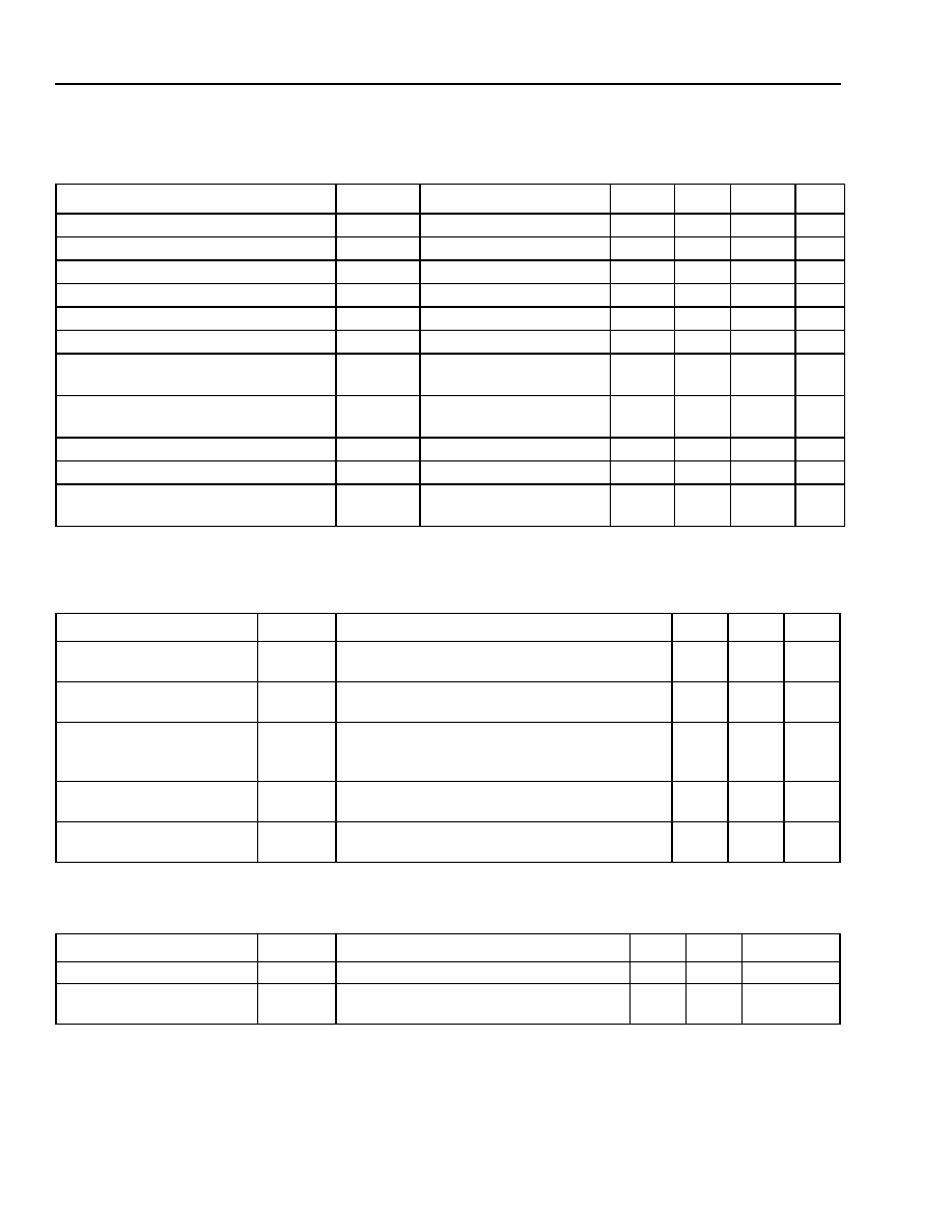
Table 6. Driver dc Data*
*VDD33 = 3.1 V—3.5 V, VDD15 = 1.4 V—1.6 V, –40 °C, and slow-fast process.
External reference, REF10 = 1.0 V ± 3%, REF14 = 1.4 V ± 3%.
Table 7. Driver ac Data*
*VDD33 = 3.1 V—3.5 V, VDD15 = 1.4 V—1.6 V, –40 °C, and slow-fast process.
Table 8. Driver Power Consumption*
*VDD33 = 3.1 V—3.5 V, VDD15 = 1.4 V—1.6 V, –40 °C, and slow-fast process.
Parameter
Symbol
Test Conditions
Min
Typ
Max
Unit
Output Voltage High, VOA or VOB
VOH
RLOAD = 100
± 1%
——
1.475
V
Output Voltage Low, VOA or VOB
VOL
RLOAD = 100
± 1%
0.925
——
V
Output Differential Voltage
VOD
RLOAD = 100
± 1%
0.25
—
0.45
V
Output Offset Voltage
VOS
RLOAD = 100
± 1%
1.125*
—
1.275
V
Output Impedance, Differential
Ro
VCM = 1.0 V and 1.4 V
80
100
120
RO Mismatch Between A and B
RO
VCM = 1.0 V and 1.4 V
——
10
%
Change in Differential Voltage between
Complementary States
VOD
RLOAD = 100
± 1%
——
25
mV
Change in Output Offset Voltage
Between Complementary States
VOS
RLOAD = 100
± 1%
——
25
mV
Output Current
ISA, ISB
Driver shorted to GND
——
24
mA
Output Current
ISAB
Drivers shorted together
——
12
mA
Power-off Output Leakage
|Ixa|, |Ixb|
VDD = 0 V
VPAD, VPADN = 0 V—2.5 V
——
10
mA
Parameter
Symbol
Test Conditions
Min
Max
Unit
VOD Fall Time, 80% to 20%
tF
ZL = 100
± 1%
CPAD = 3.0 pF, CPAD = 3.0 pF
100
210
ps
VOD Rise Time, 20% to 80%
tR
ZL = 100
± 1%
CPAD = 3.0 pF, CPAD = 3.0 pF
100
210
ps
Differential Skew
|tPHLA – tPLHB| or
|tPHLB – tPLHA|
tSKEW1
Any differential pair on package at 50% point
of the transition
—
50
ps
Channel-to-channel Skew
|tpDIFFm – tpDIFFn|,
tSKEW2
Any two signals on package at 0 V differential
——
ps
Propagation Delay Time
tPLH
tPHL
ZL = 100
± 1%
CPAD = 3.0 pF, CPADN = 3.0 pF
0.54
0.55
1.10
1.09
ns
Parameter
Symbol
Test Conditions
Min
Max
Unit
Driver dc Power
PDdc
ZL = 100
± 1%
—
26.0
mW
Driver ac Power
PDac
ZL = 100
± 1%
CPAD = 3.0 pF, CPADN = 3.0 pF
—
64
W/MHz
相關PDF資料 |
PDF描述 |
|---|---|
| ORLI10G-1BM416I | FPGA, 1296 CLBS, 380000 GATES, PBGA416 |
| ORLI10G-1BMN416I | FPGA, 1296 CLBS, 380000 GATES, PBGA416 |
| ORLI10G-1BM416 | FPGA, 1296 CLBS, 380000 GATES, PBGA416 |
| ORLI10G-1BM680 | FPGA, 1296 CLBS, 380000 GATES, PBGA680 |
| ORLI10G-2BM416 | FPGA, 1296 CLBS, 380000 GATES, PBGA416 |
相關代理商/技術參數(shù) |
參數(shù)描述 |
|---|---|
| ORLI10G-1BM680C | 功能描述:FPGA - 現(xiàn)場可編程門陣列 10368 LUT 316 I/O RoHS:否 制造商:Altera Corporation 系列:Cyclone V E 柵極數(shù)量: 邏輯塊數(shù)量:943 內嵌式塊RAM - EBR:1956 kbit 輸入/輸出端數(shù)量:128 最大工作頻率:800 MHz 工作電源電壓:1.1 V 最大工作溫度:+ 70 C 安裝風格:SMD/SMT 封裝 / 箱體:FBGA-256 |
| ORLI10G-1BM680I | 功能描述:FPGA - 現(xiàn)場可編程門陣列 10368 LUT 316 I/O RoHS:否 制造商:Altera Corporation 系列:Cyclone V E 柵極數(shù)量: 邏輯塊數(shù)量:943 內嵌式塊RAM - EBR:1956 kbit 輸入/輸出端數(shù)量:128 最大工作頻率:800 MHz 工作電源電壓:1.1 V 最大工作溫度:+ 70 C 安裝風格:SMD/SMT 封裝 / 箱體:FBGA-256 |
| ORLI10G-1BMN680C | 功能描述:FPGA - 現(xiàn)場可編程門陣列 10368 LUT 316 I/O RoHS:否 制造商:Altera Corporation 系列:Cyclone V E 柵極數(shù)量: 邏輯塊數(shù)量:943 內嵌式塊RAM - EBR:1956 kbit 輸入/輸出端數(shù)量:128 最大工作頻率:800 MHz 工作電源電壓:1.1 V 最大工作溫度:+ 70 C 安裝風格:SMD/SMT 封裝 / 箱體:FBGA-256 |
| ORLI10G-1BMN680I | 功能描述:FPGA - 現(xiàn)場可編程門陣列 10368 LUT 316 I/O RoHS:否 制造商:Altera Corporation 系列:Cyclone V E 柵極數(shù)量: 邏輯塊數(shù)量:943 內嵌式塊RAM - EBR:1956 kbit 輸入/輸出端數(shù)量:128 最大工作頻率:800 MHz 工作電源電壓:1.1 V 最大工作溫度:+ 70 C 安裝風格:SMD/SMT 封裝 / 箱體:FBGA-256 |
| ORLI10G-2BM680C | 功能描述:FPGA - 現(xiàn)場可編程門陣列 10368 LUT 316 I/O RoHS:否 制造商:Altera Corporation 系列:Cyclone V E 柵極數(shù)量: 邏輯塊數(shù)量:943 內嵌式塊RAM - EBR:1956 kbit 輸入/輸出端數(shù)量:128 最大工作頻率:800 MHz 工作電源電壓:1.1 V 最大工作溫度:+ 70 C 安裝風格:SMD/SMT 封裝 / 箱體:FBGA-256 |
發(fā)布緊急采購,3分鐘左右您將得到回復。