- 您現(xiàn)在的位置:買賣IC網(wǎng) > PDF目錄299575 > OR3T1256PS208I-DB (LATTICE SEMICONDUCTOR CORP) FPGA, 784 CLBS, 186000 GATES, PQFP208 PDF資料下載
參數(shù)資料
| 型號: | OR3T1256PS208I-DB |
| 廠商: | LATTICE SEMICONDUCTOR CORP |
| 元件分類: | FPGA |
| 英文描述: | FPGA, 784 CLBS, 186000 GATES, PQFP208 |
| 封裝: | PLASTIC, SQFP2-208 |
| 文件頁數(shù): | 172/203頁 |
| 文件大?。?/td> | 1368K |
| 代理商: | OR3T1256PS208I-DB |
第1頁第2頁第3頁第4頁第5頁第6頁第7頁第8頁第9頁第10頁第11頁第12頁第13頁第14頁第15頁第16頁第17頁第18頁第19頁第20頁第21頁第22頁第23頁第24頁第25頁第26頁第27頁第28頁第29頁第30頁第31頁第32頁第33頁第34頁第35頁第36頁第37頁第38頁第39頁第40頁第41頁第42頁第43頁第44頁第45頁第46頁第47頁第48頁第49頁第50頁第51頁第52頁第53頁第54頁第55頁第56頁第57頁第58頁第59頁第60頁第61頁第62頁第63頁第64頁第65頁第66頁第67頁第68頁第69頁第70頁第71頁第72頁第73頁第74頁第75頁第76頁第77頁第78頁第79頁第80頁第81頁第82頁第83頁第84頁第85頁第86頁第87頁第88頁第89頁第90頁第91頁第92頁第93頁第94頁第95頁第96頁第97頁第98頁第99頁第100頁第101頁第102頁第103頁第104頁第105頁第106頁第107頁第108頁第109頁第110頁第111頁第112頁第113頁第114頁第115頁第116頁第117頁第118頁第119頁第120頁第121頁第122頁第123頁第124頁第125頁第126頁第127頁第128頁第129頁第130頁第131頁第132頁第133頁第134頁第135頁第136頁第137頁第138頁第139頁第140頁第141頁第142頁第143頁第144頁第145頁第146頁第147頁第148頁第149頁第150頁第151頁第152頁第153頁第154頁第155頁第156頁第157頁第158頁第159頁第160頁第161頁第162頁第163頁第164頁第165頁第166頁第167頁第168頁第169頁第170頁第171頁當(dāng)前第172頁第173頁第174頁第175頁第176頁第177頁第178頁第179頁第180頁第181頁第182頁第183頁第184頁第185頁第186頁第187頁第188頁第189頁第190頁第191頁第192頁第193頁第194頁第195頁第196頁第197頁第198頁第199頁第200頁第201頁第202頁第203頁
70
Lattice Semiconductor
Data Sheet
November 2006
ORCA Series 3C and 3T FPGAs
Programmable Clock Manager (PCM)
The
ORCA programmable clock manager (PCM) is a
special function block that is used to modify or condi-
tion clock signals for optimum system performance.
Some of the functions that can be performed with the
PCM
are clock skew reduction (both internal and board
level), duty-cycle adjustment, clock delay reduction,
clock phase adjustment, and clock frequency multipli-
cation/division. Due to the different capabilities
required by customer application, each PCM contains
both a PLL (phase-locked loop) and a DLL (delayed-
locked loop) mode. By using PLC logic resources in
conjunction with the PCM, many other functions, such
as frequency synthesis, are possible.
There are two PCMs on each Series 3 device, one in
the lower left corner and one in the upper right corner.
Each can drive two different, but interrelated clock net-
works inside the FPGA. Each PCM can take a clock
input from the ExpressCLK pad in its corner or from
general routing resources. There are also two input
sources that provide feedback to the PCM from the
PLC array. One of these is a dedicated corner Express-
CLK
feedback, and the other is from general routing.
Each PCM sources two clock outputs, one to the cor-
ner ExpressCLK that feeds the CLKCNTRL blocks on
the two sides adjacent to the PCM, and one to the sys-
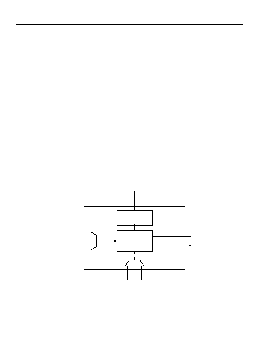
tem clock spine network through general routing. Fig-
ure 45 shows a high-level block diagram of the PCM.
Functionality of the PCM is programmed during opera-
tion through a read/write interface internal to the FPGA
array or via the conguration bit stream. The internal
FPGA interface comprises write enable and read
enable signals, a 3-bit address bus, an 8-bit input (to
the PCM) data bus, and an 8-bit output data bus. There
is also a PCM output signal, LOCK, that indicates a sta-
ble output clock state. These signals are used to pro-
gram a series of registers to congure the PCM
functional core for the desired functionality.
Operation of the PCM is divided into two modes, delay-
locked loop (DLL) and phase-locked loop (PLL). Some
operations can be performed by either mode and some
are specic to a particular mode. These will be
described in each individual mode section. In general,
DLL mode is preferable to PLL mode for the same
function because it is less sensitive to input clock
noise.
In the discussions that follow, the duty cycle is the per-
cent of the clock period during which the output clock is
high.
5-5828(F)
Figure 45. PCM Block Diagram
USER CONTROL SIGNALS
PCM-FPGA
INTERFACE
PCM CORE
FUNCTIONS
CORNER EXPRESSCLK IN
GENERAL CLOCKIN
FEEDBACK
ExpressCLK
FEEDBACK CLOCK
FROM ROUTING
EXPRESSCLK OUT
SYSTEM CLOCK OUT
(FROM GENERAL ROUTING)
(TO GENERAL ROUTING)
Select
devices
have
been
discontinued.
See
Ordering
Information
section
for
product
status.
相關(guān)PDF資料 |
PDF描述 |
|---|---|
| OR3T1256PS240-DB | FPGA, 784 CLBS, 186000 GATES, PQFP240 |
| OR3T1256PS240I-DB | FPGA, 784 CLBS, 186000 GATES, PQFP240 |
| OR3T1257PS208-DB | FPGA, 784 CLBS, 186000 GATES, PQFP208 |
| OR3T306S240I-DB | FPGA, 196 CLBS, 48000 GATES, PQFP240 |
| OR3T307S240-DB | FPGA, 196 CLBS, 48000 GATES, PQFP240 |
相關(guān)代理商/技術(shù)參數(shù) |
參數(shù)描述 |
|---|---|
| OR3T125-6PS240 | 制造商:AGERE 制造商全稱:AGERE 功能描述:3C and 3T Field-Programmable Gate Arrays |
| OR3T1256PS240-DB | 功能描述:FPGA - 現(xiàn)場可編程門陣列 6272 LUT 342 I/O RoHS:否 制造商:Altera Corporation 系列:Cyclone V E 柵極數(shù)量: 邏輯塊數(shù)量:943 內(nèi)嵌式塊RAM - EBR:1956 kbit 輸入/輸出端數(shù)量:128 最大工作頻率:800 MHz 工作電源電壓:1.1 V 最大工作溫度:+ 70 C 安裝風(fēng)格:SMD/SMT 封裝 / 箱體:FBGA-256 |
| OR3T125-6PS240I | 制造商:AGERE 制造商全稱:AGERE 功能描述:3C and 3T Field-Programmable Gate Arrays |
| OR3T1256PS240I-DB | 功能描述:FPGA - 現(xiàn)場可編程門陣列 6272 LUT 342 I/O RoHS:否 制造商:Altera Corporation 系列:Cyclone V E 柵極數(shù)量: 邏輯塊數(shù)量:943 內(nèi)嵌式塊RAM - EBR:1956 kbit 輸入/輸出端數(shù)量:128 最大工作頻率:800 MHz 工作電源電壓:1.1 V 最大工作溫度:+ 70 C 安裝風(fēng)格:SMD/SMT 封裝 / 箱體:FBGA-256 |
| OR3T125-7BA352 | 制造商:AGERE 制造商全稱:AGERE 功能描述:3C and 3T Field-Programmable Gate Arrays |
發(fā)布緊急采購,3分鐘左右您將得到回復(fù)。