- 您現(xiàn)在的位置:買賣IC網(wǎng) > PDF目錄299576 > OR3T125-4BA352I FPGA, 784 CLBS, 92000 GATES, PBGA352 PDF資料下載
參數(shù)資料
| 型號: | OR3T125-4BA352I |
| 元件分類: | FPGA |
| 英文描述: | FPGA, 784 CLBS, 92000 GATES, PBGA352 |
| 封裝: | PLASTIC, BGA-352 |
| 文件頁數(shù): | 164/210頁 |
| 文件大?。?/td> | 2138K |
| 代理商: | OR3T125-4BA352I |
第1頁第2頁第3頁第4頁第5頁第6頁第7頁第8頁第9頁第10頁第11頁第12頁第13頁第14頁第15頁第16頁第17頁第18頁第19頁第20頁第21頁第22頁第23頁第24頁第25頁第26頁第27頁第28頁第29頁第30頁第31頁第32頁第33頁第34頁第35頁第36頁第37頁第38頁第39頁第40頁第41頁第42頁第43頁第44頁第45頁第46頁第47頁第48頁第49頁第50頁第51頁第52頁第53頁第54頁第55頁第56頁第57頁第58頁第59頁第60頁第61頁第62頁第63頁第64頁第65頁第66頁第67頁第68頁第69頁第70頁第71頁第72頁第73頁第74頁第75頁第76頁第77頁第78頁第79頁第80頁第81頁第82頁第83頁第84頁第85頁第86頁第87頁第88頁第89頁第90頁第91頁第92頁第93頁第94頁第95頁第96頁第97頁第98頁第99頁第100頁第101頁第102頁第103頁第104頁第105頁第106頁第107頁第108頁第109頁第110頁第111頁第112頁第113頁第114頁第115頁第116頁第117頁第118頁第119頁第120頁第121頁第122頁第123頁第124頁第125頁第126頁第127頁第128頁第129頁第130頁第131頁第132頁第133頁第134頁第135頁第136頁第137頁第138頁第139頁第140頁第141頁第142頁第143頁第144頁第145頁第146頁第147頁第148頁第149頁第150頁第151頁第152頁第153頁第154頁第155頁第156頁第157頁第158頁第159頁第160頁第161頁第162頁第163頁當(dāng)前第164頁第165頁第166頁第167頁第168頁第169頁第170頁第171頁第172頁第173頁第174頁第175頁第176頁第177頁第178頁第179頁第180頁第181頁第182頁第183頁第184頁第185頁第186頁第187頁第188頁第189頁第190頁第191頁第192頁第193頁第194頁第195頁第196頁第197頁第198頁第199頁第200頁第201頁第202頁第203頁第204頁第205頁第206頁第207頁第208頁第209頁第210頁
Preliminary Data Sheet, Rev. 1
September 1998
ORCA Series 3 FPGAs
Lucent Technologies Inc.
57
Special Function Blocks (continued)
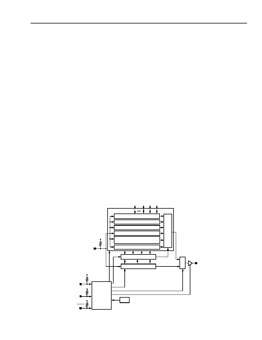
ORCA Boundary-Scan Circuitry
The
ORCA Series boundary-scan circuitry includes a
test access port controller (TAPC), instruction register
(IR), boundary-scan register (BSR), and bypass regis-
ter. It also includes circuitry to support the four pre-
defined instructions.
Figure 38 shows a functional diagram of the boundary-
scan circuitry that is implemented in the
ORCA Series.
The input pins’ (TMS, TCK, and TDI) locations vary
depending on the part, and the output pin is the dedi-
cated TDO/RD_DATA output pad. Test data in (TDI) is
the serial input data. Test mode select (TMS) controls
the boundary-scan test access port controller (TAPC).
Test clock (TCK) is the test clock on the board.
The BSR is a series connection of boundary-scan cells
(BSCs) around the periphery of the IC. Each I/O pad on
the FPGA, except for CCLK, DONE, and the boundary-
scan pins (TCK, TDI, TMS, and TDO), is included in
the BSR. The first BSC in the BSR (connected to TDI)
is located in the first PIC I/O pad on the left of the top
side of the FPGA (PTA PIC). The BSR proceeds clock-
wise around the top, right, bottom, and left sides of the
array. The last BSC in the BSR (connected to TDO) is
located on the top of the left side of the array (PL1D).
The bypass instruction uses a single FF, which resyn-
chronizes test data that is not part of the current scan
operation. In a bypass instruction, test data received on
TDI is shifted out of the bypass register to TDO. Since
the BSR (which requires a two FF delay for each pad)
is bypassed, test throughput is increased when devices
that are not part of a test operation are bypassed.
The boundary-scan logic is enabled before and during
configuration. After configuration, a configuration
option determines whether or not boundary-scan logic
is used.
The 32-bit boundary-scan identification register con-
tains the manufacturer’s ID number, unique part num-
ber, and version (as described earlier). The
identification register is the default source for data on
TDO after RESET if the TAP controller selects the shift-
data-register (SHIFT DR) instruction. If boundary scan
is not used, TMS, TDI, and TCK become user
I/Os, and TDO is 3-stated or used in the readback
operation.
An optional USERCODE is available if the boundary-
scan PSR1 instruction is not used. The selection
between PSR1 and USERCODE is a configuration
option and can be performed in
ORCA Foundry. The
USERCODE is an 11-bit value that the user can set
during device configuration and can be written to and
read from the FPGA via the boundary-scan logic. The
USERCODE value replaces the manufacturer field of
the boundary-scan ID code when the USERCODE
instruction is issued, allowing users to have configured
devices identified in a user-defined manner. The manu-
facturer ID field remains available when the IDCODE
instruction is issued.
Figure 38.
ORCA Series Boundary-Scan Circuitry Functional Diagram
TAP
CONTROLLER
TMS
TCK
BOUNDARY-SCAN REGISTER
PSR2 REGISTER (PLCs)
BYPASS REGISTER
DATA
MUX
INSTRUCTION DECODER
INSTRUCTION REGISTER
M
U
X
RESET
CLOCK IR
SHIFT IR
UPDATE IR
PUR
TDO
SELECT
ENABLE
RESET
CLOCK DR
SHIFT DR
UPDATE DR
TDI
DATA REGISTERS
PSR1/USERCODE REGISTER
CONFIGURATION REGISTER
(RAM_R, RAM_W)
PRGM
I/O BUFFERS
VDD
IDCODE REGISTER
5-5768(F)
相關(guān)PDF資料 |
PDF描述 |
|---|---|
| OR3T125-4BA352 | FPGA, 784 CLBS, 92000 GATES, PBGA352 |
| OR3T125-5B432 | FPGA, 784 CLBS, 92000 GATES, PBGA432 |
| OR3T125-5B600 | FPGA, 784 CLBS, 92000 GATES, PBGA600 |
| OR3T125-6B432 | FPGA, 784 CLBS, 92000 GATES, PBGA432 |
| OR3T125-6B600 | FPGA, 784 CLBS, 92000 GATES, PBGA600 |
相關(guān)代理商/技術(shù)參數(shù) |
參數(shù)描述 |
|---|---|
| OR3T125-4BC432I | 制造商:未知廠家 制造商全稱:未知廠家 功能描述:Field Programmable Gate Array (FPGA) |
| OR3T125-4BC600I | 制造商:未知廠家 制造商全稱:未知廠家 功能描述:Field Programmable Gate Array (FPGA) |
| OR3T125-4PS208I | 制造商:未知廠家 制造商全稱:未知廠家 功能描述:Field Programmable Gate Array (FPGA) |
| OR3T125-4PS240I | 制造商:未知廠家 制造商全稱:未知廠家 功能描述:Field Programmable Gate Array (FPGA) |
| OR3T125-5BA352 | 制造商:AGERE 制造商全稱:AGERE 功能描述:3C and 3T Field-Programmable Gate Arrays |
發(fā)布緊急采購,3分鐘左右您將得到回復(fù)。