- 您現(xiàn)在的位置:買(mǎi)賣(mài)IC網(wǎng) > PDF目錄299576 > OR3C80-5BC600I FPGA, 484 CLBS, 58000 GATES, 80 MHz, PBGA600 PDF資料下載
參數(shù)資料
| 型號(hào): | OR3C80-5BC600I |
| 元件分類(lèi): | FPGA |
| 英文描述: | FPGA, 484 CLBS, 58000 GATES, 80 MHz, PBGA600 |
| 封裝: | BGA-600 |
| 文件頁(yè)數(shù): | 172/210頁(yè) |
| 文件大小: | 2138K |
| 代理商: | OR3C80-5BC600I |
第1頁(yè)第2頁(yè)第3頁(yè)第4頁(yè)第5頁(yè)第6頁(yè)第7頁(yè)第8頁(yè)第9頁(yè)第10頁(yè)第11頁(yè)第12頁(yè)第13頁(yè)第14頁(yè)第15頁(yè)第16頁(yè)第17頁(yè)第18頁(yè)第19頁(yè)第20頁(yè)第21頁(yè)第22頁(yè)第23頁(yè)第24頁(yè)第25頁(yè)第26頁(yè)第27頁(yè)第28頁(yè)第29頁(yè)第30頁(yè)第31頁(yè)第32頁(yè)第33頁(yè)第34頁(yè)第35頁(yè)第36頁(yè)第37頁(yè)第38頁(yè)第39頁(yè)第40頁(yè)第41頁(yè)第42頁(yè)第43頁(yè)第44頁(yè)第45頁(yè)第46頁(yè)第47頁(yè)第48頁(yè)第49頁(yè)第50頁(yè)第51頁(yè)第52頁(yè)第53頁(yè)第54頁(yè)第55頁(yè)第56頁(yè)第57頁(yè)第58頁(yè)第59頁(yè)第60頁(yè)第61頁(yè)第62頁(yè)第63頁(yè)第64頁(yè)第65頁(yè)第66頁(yè)第67頁(yè)第68頁(yè)第69頁(yè)第70頁(yè)第71頁(yè)第72頁(yè)第73頁(yè)第74頁(yè)第75頁(yè)第76頁(yè)第77頁(yè)第78頁(yè)第79頁(yè)第80頁(yè)第81頁(yè)第82頁(yè)第83頁(yè)第84頁(yè)第85頁(yè)第86頁(yè)第87頁(yè)第88頁(yè)第89頁(yè)第90頁(yè)第91頁(yè)第92頁(yè)第93頁(yè)第94頁(yè)第95頁(yè)第96頁(yè)第97頁(yè)第98頁(yè)第99頁(yè)第100頁(yè)第101頁(yè)第102頁(yè)第103頁(yè)第104頁(yè)第105頁(yè)第106頁(yè)第107頁(yè)第108頁(yè)第109頁(yè)第110頁(yè)第111頁(yè)第112頁(yè)第113頁(yè)第114頁(yè)第115頁(yè)第116頁(yè)第117頁(yè)第118頁(yè)第119頁(yè)第120頁(yè)第121頁(yè)第122頁(yè)第123頁(yè)第124頁(yè)第125頁(yè)第126頁(yè)第127頁(yè)第128頁(yè)第129頁(yè)第130頁(yè)第131頁(yè)第132頁(yè)第133頁(yè)第134頁(yè)第135頁(yè)第136頁(yè)第137頁(yè)第138頁(yè)第139頁(yè)第140頁(yè)第141頁(yè)第142頁(yè)第143頁(yè)第144頁(yè)第145頁(yè)第146頁(yè)第147頁(yè)第148頁(yè)第149頁(yè)第150頁(yè)第151頁(yè)第152頁(yè)第153頁(yè)第154頁(yè)第155頁(yè)第156頁(yè)第157頁(yè)第158頁(yè)第159頁(yè)第160頁(yè)第161頁(yè)第162頁(yè)第163頁(yè)第164頁(yè)第165頁(yè)第166頁(yè)第167頁(yè)第168頁(yè)第169頁(yè)第170頁(yè)第171頁(yè)當(dāng)前第172頁(yè)第173頁(yè)第174頁(yè)第175頁(yè)第176頁(yè)第177頁(yè)第178頁(yè)第179頁(yè)第180頁(yè)第181頁(yè)第182頁(yè)第183頁(yè)第184頁(yè)第185頁(yè)第186頁(yè)第187頁(yè)第188頁(yè)第189頁(yè)第190頁(yè)第191頁(yè)第192頁(yè)第193頁(yè)第194頁(yè)第195頁(yè)第196頁(yè)第197頁(yè)第198頁(yè)第199頁(yè)第200頁(yè)第201頁(yè)第202頁(yè)第203頁(yè)第204頁(yè)第205頁(yè)第206頁(yè)第207頁(yè)第208頁(yè)第209頁(yè)第210頁(yè)
Preliminary Data Sheet, Rev. 1
ORCA Series 3 FPGAs
September 1998
64
Lucent Technologies Inc.
Microprocessor Interface (MPI) (continued)
MPI Interface to FPGA
The MPI interfaces to the user-programmable FPGA
logic using a 4-bit address, read/write control signal,
interrupt request signal, and user start and user end
handshake signals. Timing numbers are provided so
that the user-logic data transfers can be performed syn-
chronously with the host processor (
PowerPC or i960)
interface clock or asynchronously. Table 18 shows the
internal interface signals between the MPI and the
FPGA user-programmable logic. All of the signals are
connected to the MPI in the upper-left corner of the
device except for the D[7:0] and CLK signals that come
directly from the I/O pin.
The 4-bit addressing from the MPI to the PLCs allows
for up to 16 locations to be addressed by the host pro-
cessor. The user address space of the MPI does not
address any hard register. Rather, the user is free to
construct registers from FFs, latches, or RAM that can
be selected by the addressing. Alternately, the decoded
address signals may be used as control signals for
other functions such as state machines or timers.
The transaction sequence between the MPI and the
user-logic is as follows. When the host processor ini-
tiates a transaction as discussed in the preceding sec-
tions, the MPI outputs the 4-bit user address (UA[3:0])
and the read/write control signal (URDWR, which is
read-high, write-low regardless of host processor), and
then asserts the user start signal, USTART. During a
write from the host processor, the user logic can accept
data written by the host processor from the D[7:0] pins
once the USTART signal is asserted. The user logic
ends a transaction by asserting an active-high user end
(UEND) signal to the MPI.
The MPI will insert wait-states in the host processor bus
cycles, holding the host processor until the user-logic
completes its task and returns a UEND signal, upon
which the MPI generates an acknowledge signal. If the
host processor is reading from the FPGA, the user logic
must have the read data available on the D[7:0] pins of
the FPGA when the UEND signal is asserted. If the
user logic is fast or if the MPI user address is being
decoded for use as a control signal, the MPI transaction
time can be minimized by routing the USTART signal
directly to the UEND input of the MPI. The timing sec-
tion of this data sheet contains a parameter table with
delay, setup, and hold timing requirements to operate
the user-logic either synchronously or asynchronously
with the MPI host interface clock.
The user-logic may also assert an active-low interrupt
request (UIRQ) to the MPI, which, in turn, asserts an
interrupt to the host processor. Assertion of an interrupt
request is asynchronous to the host processor clock
and any read or write transaction occurring in the MPI.
The user-logic is responsible for providing any required
interrupt vectors for the host processor, and the user-
logic must deassert the interrupt request once serviced.
If the interrupt request is not deasserted in the user
logic, it will continue to be asserted to the host proces-
sor via the MPI_IRQ pin.
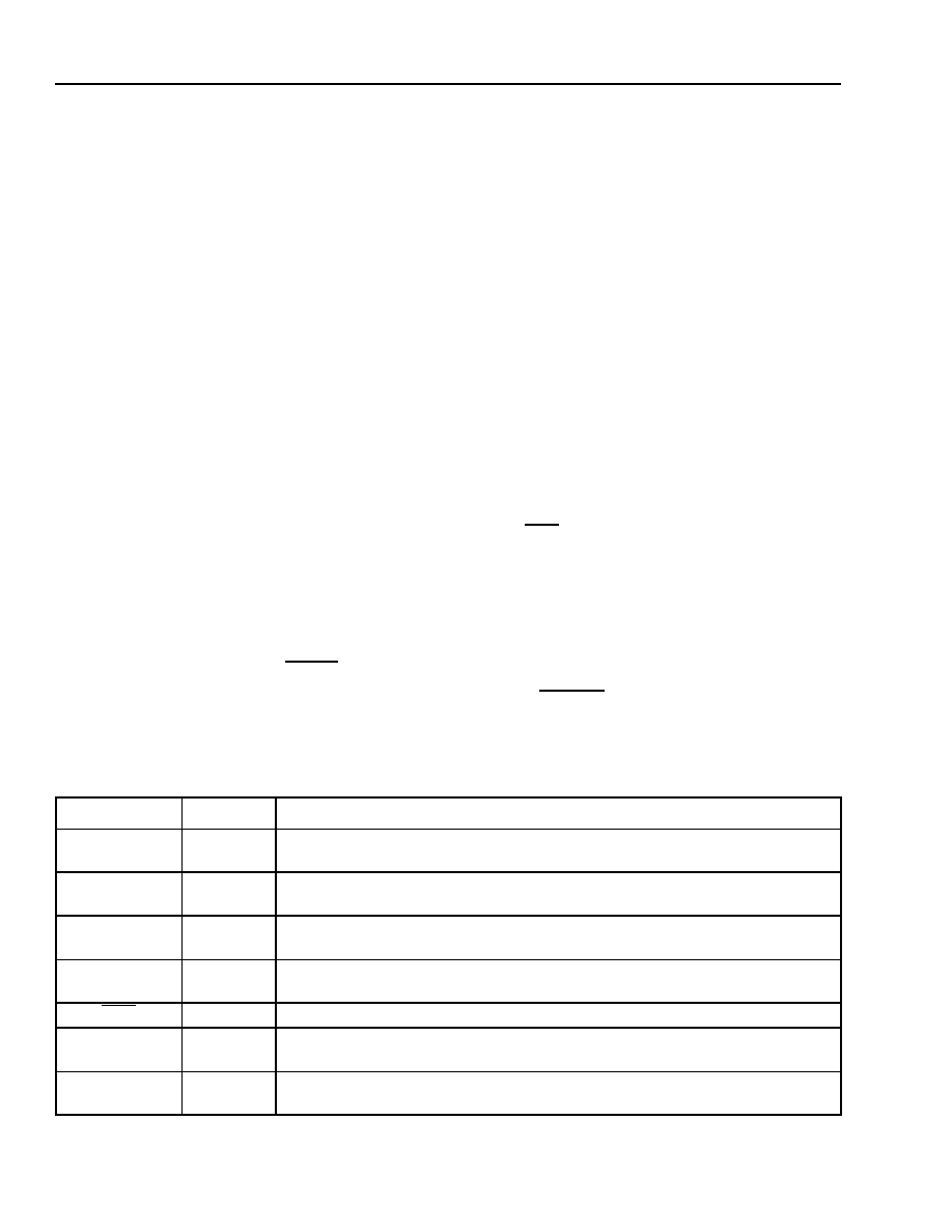
Table 18. MPI Internal Interface Signals
Signal
MPI
I/O
Function
UA[3:0]
O
User Logic Address. Addresses up to 16 unique user registers or use as control
signals.
URDWRN
O
User Logic Read/Write Control Signal. High indicates a read from user logic by
the host processor, low indicates a write to user-logic by the host processor.
USTART
O
Active-High User Start Signal. Indicates the start of an MPI transaction between
the host processor; and the user logic.
UEND
I
Active-High User End Signal. Indicates that the user-logic is finished with the
current MPI transaction.
UIRQ
I
Active-Low Interrupt. Sends request from the user-logic to the host processor.
D[7:0]
FPGA I/O
User Data. Eight data bits come directly from the FPGA pins—not through the
MPI
.
MPI_CLK
FPGA I
MPI
Clock. The MPI clock is sourced by the host processor and comes directly
from the FPGA pin—not through the MPI.
相關(guān)PDF資料 |
PDF描述 |
|---|---|
| OR3T125-4BC600I | FPGA, 784 CLBS, 92000 GATES, 80 MHz, PBGA600 |
| OR3T80-4BC600I | FPGA, 484 CLBS, 58000 GATES, 80 MHz, PBGA600 |
| OR3T80-5BC600I | FPGA, 484 CLBS, 58000 GATES, 80 MHz, PBGA600 |
| OR3T80-6BC600I | FPGA, 484 CLBS, 58000 GATES, 80 MHz, PBGA600 |
| OR3T125-4PS208I | FPGA, 784 CLBS, 92000 GATES, 80 MHz, PQFP208 |
相關(guān)代理商/技術(shù)參數(shù) |
參數(shù)描述 |
|---|---|
| OR3C805PS208 | 制造商:ORCA 功能描述:NEW |
| OR3C80-5PS208 | 制造商:AGERE 制造商全稱(chēng):AGERE 功能描述:3C and 3T Field-Programmable Gate Arrays |
| OR3C805PS208-DB | 功能描述:FPGA - 現(xiàn)場(chǎng)可編程門(mén)陣列 3872 LUT 356 I/O RoHS:否 制造商:Altera Corporation 系列:Cyclone V E 柵極數(shù)量: 邏輯塊數(shù)量:943 內(nèi)嵌式塊RAM - EBR:1956 kbit 輸入/輸出端數(shù)量:128 最大工作頻率:800 MHz 工作電源電壓:1.1 V 最大工作溫度:+ 70 C 安裝風(fēng)格:SMD/SMT 封裝 / 箱體:FBGA-256 |
| OR3C80-5PS208I | 制造商:AGERE 制造商全稱(chēng):AGERE 功能描述:3C and 3T Field-Programmable Gate Arrays |
| OR3C80-5PS240 | 制造商:AGERE 制造商全稱(chēng):AGERE 功能描述:3C and 3T Field-Programmable Gate Arrays |
發(fā)布緊急采購(gòu),3分鐘左右您將得到回復(fù)。