- 您現(xiàn)在的位置:買賣IC網(wǎng) > PDF目錄371152 > MTP3N60E (MOTOROLA INC) TMOS POWER FET 3.0 AMPERES 600 VOLTS RDS(on) = 2.2 OHMS PDF資料下載
參數(shù)資料
| 型號: | MTP3N60E |
| 廠商: | MOTOROLA INC |
| 元件分類: | JFETs |
| 英文描述: | TMOS POWER FET 3.0 AMPERES 600 VOLTS RDS(on) = 2.2 OHMS |
| 中文描述: | 3 A, 600 V, 2.2 ohm, N-CHANNEL, Si, POWER, MOSFET, TO-220AB |
| 文件頁數(shù): | 1/8頁 |
| 文件大小: | 183K |
| 代理商: | MTP3N60E |
1
Motorola, Inc. 1997
N–Channel Enhancement–Mode Silicon Gate
This advanced high voltage TMOS E–FET is designed to
withstand high energy in the avalanche mode and switch efficiently.
This new high energy device also offers a drain–to–source diode
with fast recovery time. Designed for high voltage, high speed
switching applications such as power supplies, PWM motor
controls and other inductive loads, the avalanche energy capability
is specified to eliminate the guesswork in designs where inductive
loads are switched and offer additional safety margin against
unexpected voltage transients.
Avalanche Energy Capability Specified at Elevated
Temperature
Low Stored Gate Charge for Efficient Switching
Internal Source–to–Drain Diode Designed to Replace External
Zener Transient Suppressor — Absorbs High Energy in the
Avalanche Mode
Source–to–Drain Diode Recovery Time Comparable to Discrete
Fast Recovery Diode
MAXIMUM RATINGS
(TC = 25
°
C unless otherwise noted)
Rating
Symbol
Value
Unit
Drain–Source Voltage
VDSS
VDGR
VGS
VGSM
600
Vdc
Drain–Gate Voltage (RGS = 1.0 M
)
Gate–Source Voltage — Continuous
Gate–Source Voltage
— Non–repetitive
600
Vdc
±
20
±
40
Vdc
Vpk
Drain Current — Continuous
Drain Current
— Continuous @ 100
°
C
Drain Current
— Pulsed
ID
ID
IDM
3.0
2.4
14
Adc
Total Power Dissipation @ TC = 25
°
C
Derate above 25
°
C
PD
75
0.6
Watts
W/
°
C
Operating and Storage Temperature Range
TJ, Tstg
–55 to 150
°
C
UNCLAMPED DRAIN–TO–SOURCE AVALANCHE CHARACTERISTICS
(TJ < 150
°
C)
Single Pulse Drain–to–Source Avalanche Energy — TJ = 25
°
C
Single Pulse Drain–to–Source Avalanche Energy
— TJ = 100
°
C
Repetitive Pulse Drain–to–Source Avalanche Energy
WDSR(1)
WDSR(2)
290
46
7.5
mJ
THERMAL CHARACTERISTICS
Thermal Resistance — Junction to Case
°
Thermal Resistance
— Junction to Ambient
°
R
θ
JC
R
θ
JA
TL
1.67
62.5
°
C/W
Maximum Lead Temperature for Soldering Purposes, 1/8
″
from case for 10 seconds
260
°
C
(1) VDD = 50 V, ID = 3.0 A
(2) Pulse Width and frequency is limited by TJ(max) and thermal response
Designer’s Data for “Worst Case” Conditions
— The Designer’s Data Sheet permits the design of most circuits entirely from the information presented. SOA Limit
curves — representing boundaries on device characteristics — are given to facilitate “worst case” design.
E–FET and Designer’s are trademarks of Motorola, Inc. TMOS is a registered trademark of Motorola, Inc.
Preferred
devices are Motorola recommended choices for future use and best overall value.
REV 2
Order this document
by MTP3N60E/D
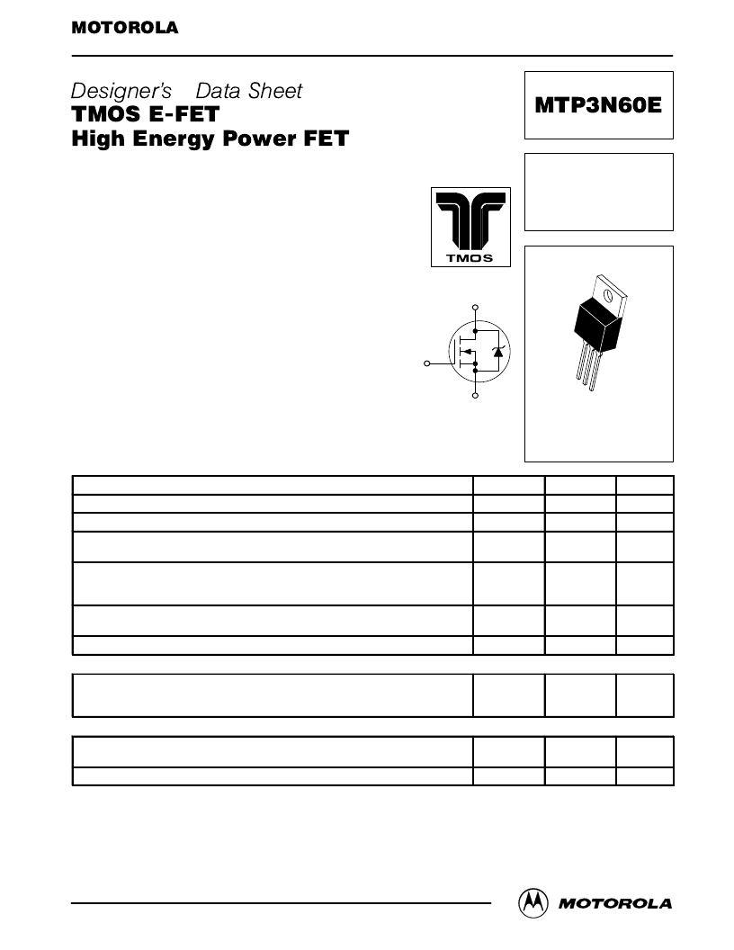
SEMICONDUCTOR TECHNICAL DATA
TMOS POWER FET
3.0 AMPERES
600 VOLTS
RDS(on) = 2.2 OHMS
D
S
G
CASE 221A–09, Style 5
TO-220AB
Motorola Preferred Device
相關(guān)PDF資料 |
PDF描述 |
|---|---|
| MTP40N10E | CONNECTOR ACCESSORY |
| MTP4N40E | TMOS POWER FET 4.0 AMPERES 400 VOLTS RDS(on) = 1.8 OHM |
| MTP4N50E | TMOS POWER FET 4.0 AMPERES 500 VOLTS RDSon = 1.5 OHMS |
| MTP50N06 | TMOS POWER FET 42 AMPERES 60 VOLTS RDS(on) = 0.028 OHM |
| MTP50N06EL | TMOS POWER FET 50 AMPERES 60 VOLTS RDS(on) = 0.028 OHM |
相關(guān)代理商/技術(shù)參數(shù) |
參數(shù)描述 |
|---|---|
| MTP3N60FI | 制造商:STMicroelectronics 功能描述:2.5 A, 600 V, 2.5 ohm, N-CHANNEL, Si, POWER, MOSFET, TO-220AB |
| MTP3NA60 | 制造商:STMicroelectronics 功能描述:3NA60 |
| MTP3-PHASE | 制造商:IRF 制造商全稱:International Rectifier 功能描述:THREE PHASE BRIDGE |
| MTP3S-E10-C | 功能描述:電纜束帶 Mutiple Tie Plate, 3 Bundle, M-S Ties, # RoHS:否 制造商:Phoenix Contact 產(chǎn)品:Cable Tie Mounts 類型:Adhesive 顏色:Black 材料:Acrylonitrile Butadiene Styrene (ABS) 長度:19 mm 寬度:19 mm 抗拉強度: |
| MTP3S-E10-C39 | 功能描述:電纜束帶 Mutiple Tie Plate, 3 Bundle, M-S Ties, # RoHS:否 制造商:Phoenix Contact 產(chǎn)品:Cable Tie Mounts 類型:Adhesive 顏色:Black 材料:Acrylonitrile Butadiene Styrene (ABS) 長度:19 mm 寬度:19 mm 抗拉強度: |
發(fā)布緊急采購,3分鐘左右您將得到回復(fù)。