- 您現(xiàn)在的位置:買(mǎi)賣(mài)IC網(wǎng) > PDF目錄371152 > MTP3N50E (MOTOROLA INC) TMOS POWER FET 3.0 AMPERES 500 VOLTS RDS(on) = 3.0 OHMS PDF資料下載
參數(shù)資料
| 型號(hào): | MTP3N50E |
| 廠商: | MOTOROLA INC |
| 元件分類(lèi): | JFETs |
| 英文描述: | TMOS POWER FET 3.0 AMPERES 500 VOLTS RDS(on) = 3.0 OHMS |
| 中文描述: | 3 A, 500 V, 3 ohm, N-CHANNEL, Si, POWER, MOSFET, TO-220AB |
| 文件頁(yè)數(shù): | 5/8頁(yè) |
| 文件大小: | 251K |
| 代理商: | MTP3N50E |
I
Figure 12. Commutating Safe Operating Area (CSOA)
0
100
VDS, DRAIN-TO-SOURCE VOLTAGE (VOLTS)
200
300
400
4
3
2
0
1
+
+
–
Figure 13. Commutating Safe Operating Area
Test Circuit
VR
VGS
IFM
20 V
RGS
DUT
IS
Li
VR = 80% OF RATED VDS
VdsL = Vf + Li
dls/dt
–
di/dt
≤
50 A/
μ
s
500
600
Figure 14. Unclamped Inductive Switching
Test Circuit
Figure 15. Unclamped Inductive Switching
Waveforms
t
L
VDS
ID
VDD
tP
V(BR)DSS
VDD
ID(t)
C
4700
μ
F
250 V
RGS
50
IO
Vds(t)
t, (TIME)
WDSR
1
2
L IO2
V(BR)DSS
V(BR)DSS– VDD
VDS
5
Motorola TMOS Power MOSFET Transistor Device Data
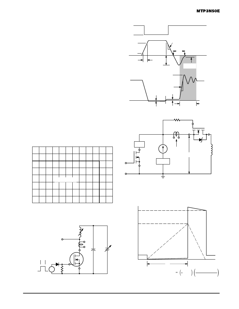
COMMUTATING SAFE OPERATING AREA (CSOA)
The Commutating Safe Operating Area (CSOA) of
Figure 12 defines the limits of safe operation for commutated
source-drain current versus re-applied drain voltage when
the source-drain diode has undergone forward bias. The
curve shows the limitations of IFM and peak VR for a given
commutation speed. It is applicable when waveforms similar
to those of Figure 11 are present. Full or half-bridge PWM DC
motor controllers are common applications requiring CSOA
data.
The time interval tfrr is the speed of the commutation cycle.
Device stresses increase with commutation speed, so tfrr is
specified with a minimum value. Faster commutation speeds
require an appropriate derating of IFM, peak VR or both. Ulti-
mately, tfrr is limited primarily by device, package, and circuit
impedances. Maximum device stress occurs during trr as the
diode goes from conduction to reverse blocking.
VDS(pk) is the peak drain–to–source voltage that the device
must sustain during commutation; IFM is the maximum for-
ward source-drain diode current just prior to the onset of
commutation.
VR is specified at 80% of V(BR)DSS to ensure that the
CSOA stress is maximized as IS decays from IRM to zero.
RGS should be minimized during commutation. TJ has only
a second order effect on CSOA.
Stray inductances, Li in Motorola’s test circuit are assumed
to be practical minimums.
Figure 11. Commutating Waveforms
15 V
VGS
0
90%
IFM
dls/dt
IS
10%
trr
IRM
ton
VDS
Vf
VdsL
dVDS/dt
VDS(pk)
MAX. CSOA
STRESS AREA
VR
0.25 IRM
相關(guān)PDF資料 |
PDF描述 |
|---|---|
| MTP3N50 | TMOS POWER FET 3.0 AMPERES 500 VOLTS RDS(on) = 3.0 OHMS |
| MTP3N60E | TMOS POWER FET 3.0 AMPERES 600 VOLTS RDS(on) = 2.2 OHMS |
| MTP40N10E | CONNECTOR ACCESSORY |
| MTP4N40E | TMOS POWER FET 4.0 AMPERES 400 VOLTS RDS(on) = 1.8 OHM |
| MTP4N50E | TMOS POWER FET 4.0 AMPERES 500 VOLTS RDSon = 1.5 OHMS |
相關(guān)代理商/技術(shù)參數(shù) |
參數(shù)描述 |
|---|---|
| MTP3N55 | 制造商:未知廠家 制造商全稱:未知廠家 功能描述:HIGH VOLTAGE POWER MOSFET N-CHANNEL |
| MTP3N60 | 制造商:STMICROELECTRONICS 制造商全稱:STMicroelectronics 功能描述:N - CHANNEL ENHANCEMENT MODE POWER MOS TRANSISTOR |
| MTP3N60E | 制造商:ON Semiconductor 功能描述:Trans MOSFET N-CH 600V 3A 3-Pin(3+Tab) TO-220 制造商:ON Semiconductor 功能描述:TMO SPWR 600V .5R TO220 制造商:ON Semiconductor 功能描述:MOSFET Transistor, N-Channel, TO-220 制造商:Motorola Inc 功能描述: 制造商:MOTOROLA 功能描述: |
| MTP3N60FI | 制造商:STMicroelectronics 功能描述:2.5 A, 600 V, 2.5 ohm, N-CHANNEL, Si, POWER, MOSFET, TO-220AB |
| MTP3NA60 | 制造商:STMicroelectronics 功能描述:3NA60 |
發(fā)布緊急采購(gòu),3分鐘左右您將得到回復(fù)。