- 您現(xiàn)在的位置:買賣IC網(wǎng) > PDF目錄371151 > MTD6N15 (MOTOROLA INC) TMOS POWER FET 6.0 AMPERES 150 VOLTS RDS(on) = 0.3 OHM PDF資料下載
參數(shù)資料
| 型號: | MTD6N15 |
| 廠商: | MOTOROLA INC |
| 元件分類: | JFETs |
| 英文描述: | TMOS POWER FET 6.0 AMPERES 150 VOLTS RDS(on) = 0.3 OHM |
| 中文描述: | 6 A, 150 V, 0.3 ohm, N-CHANNEL, Si, POWER, MOSFET, TO-252 |
| 文件頁數(shù): | 1/10頁 |
| 文件大小: | 231K |
| 代理商: | MTD6N15 |
1
Motorola, Inc. 1996
N–Channel Enhancement–Mode Silicon Gate
This TMOS Power FET is designed for high speed, low loss
power switching applications such as switching regulators, convert-
ers, solenoid and relay drivers.
Silicon Gate for Fast Switching Speeds
Low RDS(on) — 0.3
Max
Rugged — SOA is Power Dissipation Limited
Source–to–Drain Diode Characterized for Use With
Inductive Loads
Low Drive Requirement — VGS(th) = 4.0 V Max
Surface Mount Package on 16 mm Tape
MAXIMUM RATINGS
Rating
Symbol
Value
Unit
Drain–Source Voltage
VDSS
VDGR
VGS
VGSM
150
Vdc
Drain–Gate Voltage (RGS = 1.0 M
)
Gate–Source Voltage — Continuous
Gate–Source Voltage
— Non–Repetitive (tp
≤
50
μ
s)
150
Vdc
±
20
±
40
Vdc
Vpk
Drain Current — Continuous
Drain Current
— Pulsed
ID
IDM
6.0
20
Adc
Total Power Dissipation @ TC = 25
°
C
Derate above 25
°
C
PD
20
0.16
Watts
W/
°
C
Total Power Dissipation @ TA = 25
°
C
Derate above 25
°
C
PD
1.25
0.01
Watts
W/
°
C
Total Power Dissipation @ TA = 25
°
C (1)
Derate above 25
°
C
PD
1.75
0.014
Watts
W/
°
C
Operating and Storage Junction Temperature Range
TJ, Tstg
–65 to +150
°
C
THERMAL CHARACTERISTICS
Thermal Resistance — Junction to Case
Thermal Resistance
— Junction to Ambient
Thermal Resistance
— Junction to Ambient (1)
R
θ
JC
R
θ
JA
R
θ
JA
6.25
100
71.4
°
C/W
ELECTRICAL CHARACTERISTICS
(TJ = 25
°
C unless otherwise noted)
Characteristic
Symbol
Min
Max
Unit
OFF CHARACTERISTICS
Drain–Source Breakdown Voltage
(VGS = 0 Vdc, ID = 0.25 mAdc)
V(BR)DSS
150
—
Vdc
Zero Gate Voltage Drain Current
(VDS = Rated VDSS, VGS = 0 Vdc)
TJ = 125
°
C
(1) These ratings are applicable when surface mounted on the minimum pad size recommended.
IDSS
—
—
10
100
μ
Adc
(continued)
Designer’s Data for “Worst Case” Conditions
— The Designer’s Data Sheet permits the design of most circuits entirely from the information presented. SOA Limit
curves — representing boundaries on device characteristics — are given to facilitate “worst case” design.
Designer’s is a trademark of Motorola, Inc. TMOS is a registered trademark of Motorola, Inc.
Order this document
by MTD6N15/D
SEMICONDUCTOR TECHNICAL DATA
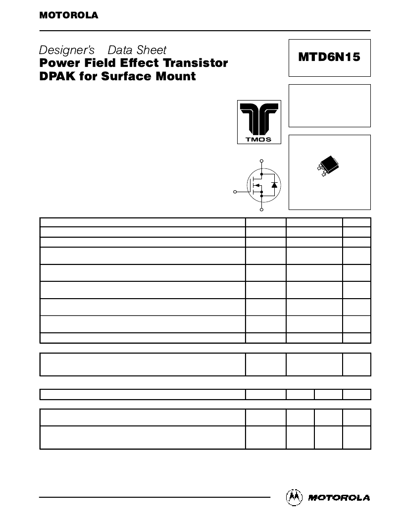
CASE 369A–13, Style 2
DPAK (TO–252)
TMOS POWER FET
6.0 AMPERES
150 VOLTS
RDS(on) = 0.3 OHM
D
S
G
相關(guān)PDF資料 |
PDF描述 |
|---|---|
| MTD6N15T4 | Power Field Effect Transistor DPAK for Surface Mount |
| MTD6N15-1 | Power Field Effect Transistor DPAK for Surface Mount |
| MTD8N06E | TMOS POWER FET 8.0 AMPERES 60 VOLTS RDS(on) = 0.12 OHM |
| MTD9N10E | TMOS POWER FET 9.0 AMPERES 100 VOLTS RDS(on) = 0.25 OHM |
| MTDF1N02HD | DUAL TMOS POWER MOSFET 1.7 AMPERES 20 VOLTS RDS(on) = 0.120 OHM |
相關(guān)代理商/技術(shù)參數(shù) |
參數(shù)描述 |
|---|---|
| MTD6N15-1 | 制造商:ONSEMI 制造商全稱:ON Semiconductor 功能描述:Power Field Effect Transistor DPAK for Surface Mount |
| MTD6N15T4 | 功能描述:MOSFET 150V 6A N-Channel RoHS:否 制造商:STMicroelectronics 晶體管極性:N-Channel 汲極/源極擊穿電壓:650 V 閘/源擊穿電壓:25 V 漏極連續(xù)電流:130 A 電阻汲極/源極 RDS(導(dǎo)通):0.014 Ohms 配置:Single 最大工作溫度: 安裝風格:Through Hole 封裝 / 箱體:Max247 封裝:Tube |
| MTD6N15T4G | 功能描述:MOSFET NFET DPAK 150V 6A 300mOhm RoHS:否 制造商:STMicroelectronics 晶體管極性:N-Channel 汲極/源極擊穿電壓:650 V 閘/源擊穿電壓:25 V 漏極連續(xù)電流:130 A 電阻汲極/源極 RDS(導(dǎo)通):0.014 Ohms 配置:Single 最大工作溫度: 安裝風格:Through Hole 封裝 / 箱體:Max247 封裝:Tube |
| MTD6N15T4GV | 功能描述:MOSFET Single N-Ch 150V 6A RoHS:否 制造商:STMicroelectronics 晶體管極性:N-Channel 汲極/源極擊穿電壓:650 V 閘/源擊穿電壓:25 V 漏極連續(xù)電流:130 A 電阻汲極/源極 RDS(導(dǎo)通):0.014 Ohms 配置:Single 最大工作溫度: 安裝風格:Through Hole 封裝 / 箱體:Max247 封裝:Tube |
| MTD6N20 | 制造商:ON Semiconductor 功能描述:MOSFET N D-PAK |
發(fā)布緊急采購,3分鐘左右您將得到回復(fù)。