- 您現(xiàn)在的位置:買賣IC網(wǎng) > PDF目錄385641 > MTB2P50E (ON SEMICONDUCTOR) Power MOSFET 2 Amps, 500 Volts(2A, 500V功率MOSFET) PDF資料下載
參數(shù)資料
| 型號(hào): | MTB2P50E |
| 廠商: | ON SEMICONDUCTOR |
| 元件分類: | 功率晶體管 |
| 英文描述: | Power MOSFET 2 Amps, 500 Volts(2A, 500V功率MOSFET) |
| 中文描述: | 2 A, 500 V, 6 ohm, P-CHANNEL, Si, POWER, MOSFET |
| 封裝: | CASE 418B-04, D2PAK-3 |
| 文件頁(yè)數(shù): | 4/8頁(yè) |
| 文件大?。?/td> | 85K |
| 代理商: | MTB2P50E |
MTB2P50E
http://onsemi.com
4
POWER MOSFET SWITCHING
Switching behavior is most easily modeled and predicted
by recognizing that the power MOSFET is charge
controlled. The lengths of various switching intervals ( t)
are determined by how fast the FET input capacitance can
be charged by current from the generator.
The published capacitance data is difficult to use for
calculating rise and fall because draingate capacitance
varies greatly with applied voltage. Accordingly, gate
charge data is used. In most cases, a satisfactory estimate of
average input current (I
G(AV)
) can be made from a
rudimentary analysis of the drive circuit so that
t = Q/I
G(AV)
During the rise and fall time interval when switching a
resistive load, V
GS
remains virtually constant at a level
known as the plateau voltage, V
SGP
. Therefore, rise and fall
times may be approximated by the following:
t
r
= Q
2
x R
G
/(V
GG
V
GSP
)
t
f
= Q
2
x R
G
/V
GSP
where
V
GG
= the gate drive voltage, which varies from zero to V
GG
R
G
= the gate drive resistance
and Q
2
and V
GSP
are read from the gate charge curve.
During the turnon and turnoff delay times, gate current is
not constant. The simplest calculation uses appropriate
values from the capacitance curves in a standard equation for
voltage change in an RC network. The equations are:
t
d(on)
= R
G
C
iss
In [V
GG
/(V
GG
V
GSP
)]
t
d(off)
= R
G
C
iss
In (V
GG
/V
GSP
)
The capacitance (C
iss
) is read from the capacitance curve at
a voltage corresponding to the offstate condition when
calculating t
d(on)
and is read at a voltage corresponding to the
onstate when calculating t
d(off)
.
At high switching speeds, parasitic circuit elements
complicate the analysis. The inductance of the MOSFET
source lead, inside the package and in the circuit wiring which
is common to both the drain and gate current paths, produces
a voltage at the source which reduces the gate drive current.
The voltage is determined by Ldi/dt, but since di/dt is a
function of drain current, the mathematical solution is
complex. The MOSFET output capacitance also complicates
the mathematics. And finally, MOSFETs have finite internal
gate resistance which effectively adds to the resistance of the
driving source, but the internal resistance is difficult to
measure and, consequently, is not specified.
The resistive switching time variation versus gate
resistance (Figure 9) shows how typical switching
performance is affected by the parasitic circuit elements. If
the parasitics were not present, the slope of the curves would
maintain a value of unity regardless of the switching speed.
The circuit used to obtain the data is constructed to minimize
common inductance in the drain and gate circuit loops and
is believed readily achievable with board mounted
components. Most power electronic loads are inductive; the
data in the figure is taken with a resistive load, which
approximates an optimally snubbed inductive load. Power
MOSFETs may be safely operated into an inductive load;
however, snubbing reduces switching losses.
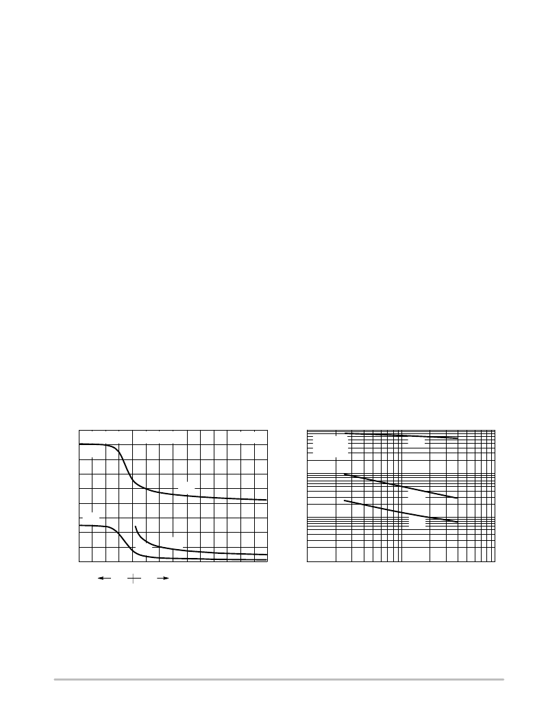
GATETOSOURCE OR DRAINTOSOURCE VOLTAGE (VOLTS)
C
Figure 7a. Capacitance Variation
1800
1600
1400
1200
1000
800
600
0
V
GS
V
DS
Figure 7b. High Voltage Capacitance
Variation
V
DS
, DRAINTOSOURCE VOLTAGE (VOLTS)
1000
100
10
1
C
V
GS
= 0 V
10
5
0
5
10
15
20
25
C
rss
C
iss
C
iss
C
oss
C
rss
10
100
1000
C
iss
C
oss
C
rss
V
GS
= 0 V
T
J
= 25
°
C
400
200
V
DS
= 0 V
T
J
= 25
°
C
相關(guān)PDF資料 |
PDF描述 |
|---|---|
| MTB50P03HDL | Power MOSFET 50 Amps, 30 Volts, Logic Level(50A, 30V, D2PAK, P溝道功率MOSFET) |
| MTD20N06HDLT4 | Power MOSFET 20 Amps, 60 Volts, Logic Level N−Channel DPAK |
| MTD20N06HDLT4G | Power MOSFET 20 Amps, 60 Volts, Logic Level N−Channel DPAK |
| MTD6N15 | Power Field Effect Transistor DPAK for Surface Mount(功率場(chǎng)效應(yīng)晶體管) |
| MTD6N20E | Power MOSFET 6 Amps, 200 Volts(6A, 200V功率MOSFET) |
相關(guān)代理商/技術(shù)參數(shù) |
參數(shù)描述 |
|---|---|
| MTB2P50ET4 | 制造商:ONSEMI 制造商全稱:ON Semiconductor 功能描述:Power MOSFET 2 Amps, 500 Volts P−Channel D2PAK |
| MTB2P50ET4G | 功能描述:MOSFET PFET 500V 2A 6O RoHS:否 制造商:STMicroelectronics 晶體管極性:N-Channel 汲極/源極擊穿電壓:650 V 閘/源擊穿電壓:25 V 漏極連續(xù)電流:130 A 電阻汲極/源極 RDS(導(dǎo)通):0.014 Ohms 配置:Single 最大工作溫度: 安裝風(fēng)格:Through Hole 封裝 / 箱體:Max247 封裝:Tube |
| MTB306D | 功能描述:撥動(dòng)開(kāi)關(guān) 3PDT TOGGLE SWITCH Long Bat Actuator RoHS:否 制造商:C&K Components 觸點(diǎn)形式:DPDT 開(kāi)關(guān)功能:ON - ON - ON 電流額定值: 電壓額定值 AC:20 V 電壓額定值 DC:20 V 功率額定值:0.4 VA 端接類型:V-Bracket 安裝風(fēng)格: 端子密封:Epoxy 觸點(diǎn)電鍍:Gold 照明:Not Illuminated |
| MTB306D04 | 制造商:TE Connectivity 功能描述:Switch Toggle ON None ON 3PDT Bat Toggle Wire Lug 6A 250VAC 28VDC Panel Mount with Threads |
| MTB30HA | 制造商:未知廠家 制造商全稱:未知廠家 功能描述:Full-Size (7.3mm or 4.7mm height) |
發(fā)布緊急采購(gòu),3分鐘左右您將得到回復(fù)。