- 您現(xiàn)在的位置:買(mǎi)賣(mài)IC網(wǎng) > PDF目錄385640 > MT4LC4M16F5 (Micron Technology, Inc.) DRAM PDF資料下載
參數(shù)資料
| 型號(hào): | MT4LC4M16F5 |
| 廠商: | Micron Technology, Inc. |
| 英文描述: | DRAM |
| 中文描述: | 內(nèi)存 |
| 文件頁(yè)數(shù): | 3/19頁(yè) |
| 文件大小: | 339K |
| 代理商: | MT4LC4M16F5 |
第1頁(yè)第2頁(yè)當(dāng)前第3頁(yè)第4頁(yè)第5頁(yè)第6頁(yè)第7頁(yè)第8頁(yè)第9頁(yè)第10頁(yè)第11頁(yè)第12頁(yè)第13頁(yè)第14頁(yè)第15頁(yè)第16頁(yè)第17頁(yè)第18頁(yè)第19頁(yè)

3
4 Meg x 16 FPM DRAM
D28_2.p65 – Rev. 5/00
Micron Technology, Inc., reserves the right to change products or specifications without notice.
2000, Micron Technology, Inc.
4 MEG x 16
FPM DRAM
STORED
DATA
1
1
0
1
1
1
1
1
RAS#
CASL#
WE#
X = NOT EFFECTIVE (DON'T CARE)
ADDRESS 1
ADDRESS 0
0
1
0
1
0
0
0
0
WORD WRITE
LOWER BYTE WRITE
CASH#
INPUT
DATA
0
0
1
0
0
0
0
0
1
0
1
0
1
1
1
1
X
X
X
X
X
X
X
X
INPUT
DATA
1
1
0
1
1
1
1
1
INPUT
DATA
STORED
DATA
1
1
0
1
1
1
1
1
INPUT
DATA
STORED
DATA
0
0
1
0
0
0
0
0
1
0
1
0
1
1
1
1
STORED
DATA
0
0
1
0
0
0
0
0
1
0
1
0
1
1
1
1
X
X
X
X
X
X
X
X
1
0
1
0
1
1
1
1
UPPER BYTE
(DQ8-DQ15)
OF WORD
LOWER BYTE
(DQ0-DQ7)
OF WORD
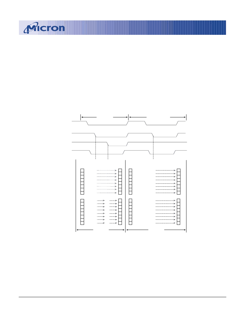
Figure 1
WORD and BYTE WRITE Example
DRAM REFRESH
The supply voltage must be maintained at the speci-
fied levels, and the refresh requirements must be met in
order to retain stored data in the DRAM. The refresh
requirements are met by refreshing all rows in the
DRAM array at least once every 64ms. The recom-
mended procedure is to execute 4,096 CBR REFRESH
cycles, either uniformly spaced or grouped in bursts,
every 64ms. The MT4LC4M16F5 internally refreshes
one row for every CBR cycle, so executing 4,096 CBR
cycles covers all rows. The CBR REFRESH will invoke the
internal refresh counter for automatic RAS# address-
ing. Alternatively, RAS#-ONLY REFRESH capability is
inherently provided. However, with this method some
compatibility issues may become apparent. JEDEC
strongly recommends the use of CBR REFRESH for this
device.
STANDBY
Returning RAS# and CAS# HIGH terminates a
memory cycle and decreases chip current to a reduced
standby level. The chip is preconditioned for the next
cycle during the RAS# HIGH time.
相關(guān)PDF資料 |
PDF描述 |
|---|---|
| MT4LC4M16R6 | DRAM |
| MT4LC8M8E1TG-5 | DRAM |
| MT4LC8M8E1TG-5S | PLUG, LOW PROFILE 3 POLE |
| MT4LC8M8P4DJ-5 | DRAM |
| MT4LC8M8P4DJ-6 | DRAM |
相關(guān)代理商/技術(shù)參數(shù) |
參數(shù)描述 |
|---|---|
| MT4LC4M16N3TG-5 | 制造商:MICRON 制造商全稱(chēng):Micron Technology 功能描述:DRAM |
| MT4LC4M16N3TG-5S | 制造商:MICRON 制造商全稱(chēng):Micron Technology 功能描述:DRAM |
| MT4LC4M16N3TG-6 | 制造商:MICRON 制造商全稱(chēng):Micron Technology 功能描述:DRAM |
| MT4LC4M16N3TG-6S | 制造商:MICRON 制造商全稱(chēng):Micron Technology 功能描述:DRAM |
| MT4LC4M16R6 | 制造商:MICRON 制造商全稱(chēng):Micron Technology 功能描述:DRAM |
發(fā)布緊急采購(gòu),3分鐘左右您將得到回復(fù)。