- 您現(xiàn)在的位置:買(mǎi)賣(mài)IC網(wǎng) > PDF目錄385640 > MT4LC4M16R6 (Micron Technology, Inc.) DRAM PDF資料下載
參數(shù)資料
| 型號(hào): | MT4LC4M16R6 |
| 廠(chǎng)商: | Micron Technology, Inc. |
| 英文描述: | DRAM |
| 中文描述: | 內(nèi)存 |
| 文件頁(yè)數(shù): | 1/19頁(yè) |
| 文件大小: | 339K |
| 代理商: | MT4LC4M16R6 |
當(dāng)前第1頁(yè)第2頁(yè)第3頁(yè)第4頁(yè)第5頁(yè)第6頁(yè)第7頁(yè)第8頁(yè)第9頁(yè)第10頁(yè)第11頁(yè)第12頁(yè)第13頁(yè)第14頁(yè)第15頁(yè)第16頁(yè)第17頁(yè)第18頁(yè)第19頁(yè)
1
4 Meg x 16 FPM DRAM
D28_2.p65 – Rev. 5/00
Micron Technology, Inc., reserves the right to change products or specifications without notice.
2000, Micron Technology, Inc.
4 MEG x 16
FPM DRAM
FEATURES
Single +3.3V ±0.3V power supply
Industry-standard x16 pinout, timing, functions,
and packages
12 row, 10 column addresses
High-performance CMOS silicon-gate process
All inputs, outputs and clocks are LVTTL-compatible
FAST PAGE MODE (FPM) access
4,096-cycle CAS#-BEFORE-RAS# (CBR) REFRESH
distributed across 64ms
OPTIONS
Plastic Package
50-pin TSOP (400 mil)
MARKING
TG
Timing
50ns access
60ns access
-5
-6
Refresh Rate
Standard Refresh
None
Part Number Example
MT4LC4M16F5TG-5
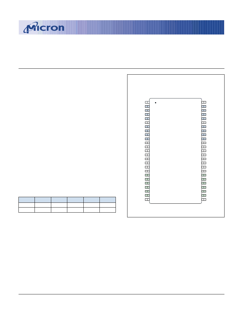
PIN ASSIGNMENT (Top View )
DRAM
MT4LC4M16F5
Web site: www.micron.com/mti/msp/html/50-Pin TSOPKEY TIMING PARAMETERS
SPEED
-5
-6
t
RC
90ns
110ns
t
RAC
50ns
60ns
t
PC
30ns
35ns
t
AA
25ns
30ns
t
CAC
13ns
15ns
V
CC
DQ0
DQ1
DQ2
DQ3
V
CC
DQ4
DQ5
DQ6
DQ7
NC
V
CC
WE#
RAS#
NC
NC
NC
NC
A0
A1
A2
A3
A4
A5
V
CC
1
2
3
4
5
6
7
8
9
10
11
12
13
14
15
16
17
18
19
20
21
22
23
24
25
50
49
48
47
46
45
44
43
42
41
40
39
38
37
36
35
34
33
32
31
30
29
28
27
26
V
SS
DQ15
DQ14
DQ13
DQ12
V
SS
DQ11
DQ10
DQ9
DQ8
NC
V
SS
CASL#
CASH#
OE#
NC
NC
NC
A11
A10
A9
A8
A7
A6
V
SS
GENERAL DESCRIPTION
The 4 Meg x 16 DRAM is a high-speed CMOS,
dynamic random-access memory device containing
67,108,864 bits organized in a x16 configuration. The
MT4LC4M16F5 is functionally organized as 4,194,304
locations containing 16 bits each. The 4,194,304
memory locations are arranged in 4,096 rows by 1,024
columns. During READ or WRITE cycles, each location
is uniquely addressed via the address bits: 12 row-
address bits (A0-A11) and 10 column-address bits (A0-
A9). In addition, both byte and word accesses are
supported via the two CAS# pins (CASL# and CASH#).
The CAS# functionality and timing related to address
and control functions (e.g., latching column addresses
or selecting CBR REFRESH) are such that the internal
CAS# signal is determined by the first external CAS#
signal (CASL# or CASH#) to transition LOW and the last
to transition back HIGH. The CAS# functionality and
timing related to driving or latching data are such that
each CAS# signal independently controls the associ-
ated eight DQ pins.
The row address is latched by the RAS# signal, then
the column address by CAS#. The device provides FAST-
PAGE-MODE operation, allowing for fast successive
data operations (READ, WRITE, or READ-MODIFY-
WRITE) within a given row.
The MT4LC4M16F5 must be refreshed periodi-
cally in order to retain stored data.
NOTE:
1. The # symbol indicates signal is active LOW.
相關(guān)PDF資料 |
PDF描述 |
|---|---|
| MT4LC8M8E1TG-5 | DRAM |
| MT4LC8M8E1TG-5S | PLUG, LOW PROFILE 3 POLE |
| MT4LC8M8P4DJ-5 | DRAM |
| MT4LC8M8P4DJ-6 | DRAM |
| MT4LC8M8P4TG-5 | DRAM |
相關(guān)代理商/技術(shù)參數(shù) |
參數(shù)描述 |
|---|---|
| MT4LC4M16R6-1 | 制造商:MICRON 制造商全稱(chēng):Micron Technology 功能描述:DRAM |
| MT4LC4M16R6TG5 | 制造商:Micron Technology Inc 功能描述: |
| MT4LC4M16R6TG-5 | 制造商:Micron Technology Inc 功能描述: |
| MT4LC4M16R6TG-5S | 制造商:MICRON 制造商全稱(chēng):Micron Technology 功能描述:DRAM |
發(fā)布緊急采購(gòu),3分鐘左右您將得到回復(fù)。