- 您現(xiàn)在的位置:買賣IC網(wǎng) > PDF目錄385639 > MT46V2M32V1 (Micron Technology, Inc.) DOUBLE DATA RATE DDR SDRAM PDF資料下載
參數(shù)資料
| 型號(hào): | MT46V2M32V1 |
| 廠商: | Micron Technology, Inc. |
| 英文描述: | DOUBLE DATA RATE DDR SDRAM |
| 中文描述: | 雙倍數(shù)據(jù)速率的DDR SDRAM內(nèi)存 |
| 文件頁數(shù): | 54/65頁 |
| 文件大小: | 2360K |
| 代理商: | MT46V2M32V1 |
第1頁第2頁第3頁第4頁第5頁第6頁第7頁第8頁第9頁第10頁第11頁第12頁第13頁第14頁第15頁第16頁第17頁第18頁第19頁第20頁第21頁第22頁第23頁第24頁第25頁第26頁第27頁第28頁第29頁第30頁第31頁第32頁第33頁第34頁第35頁第36頁第37頁第38頁第39頁第40頁第41頁第42頁第43頁第44頁第45頁第46頁第47頁第48頁第49頁第50頁第51頁第52頁第53頁當(dāng)前第54頁第55頁第56頁第57頁第58頁第59頁第60頁第61頁第62頁第63頁第64頁第65頁
54
64Mb: x32 DDR SDRAM
2M32DDR-07.p65
–
Rev. 12/01
Micron Technology, Inc., reserves the right to change products or specifications without notice.
2001, Micron Technology, Inc.
64Mb: x32
DDR SDRAM
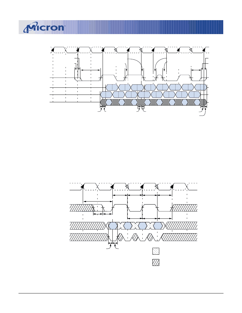
Figure 30
Data Input Timing
Figure 29
Data Output Timing
–
t
AC and
t
DQSCK
CK
CK#
DQS
T0
7
T1
T2
T3
T4
T5
T2n
T3n
T4n
T5n
T6
NOTE:
1.tDQSCK is the DQS output window relative to CK and is the
“
long term
”
component of DQS skew.
2.
DQs transitioning after DQS transition define tDQSQ window.
3. All DQs must transition by tDQSQ after DQS transitions, regardless of tAC.
4.tAC is the DQ output window relative to CK, and is the
“
long term
”
component of DQ skew.
5.tLZ(
MIN
), tAC(
MIN
) and tHZ(
MIN
) are the first valid signal transition.
6.tLZ(
MAX
), tAC(
MAX
) and tHZ(
MAX
) are the latest valid signal transition.
7. READ command with CL = 2 issued at T0.
tRPST
tLZ(MAX)
tLZ(MIN)
tDQSCK
1
(MAX)
tDQSCK
1
(MIN)
tDQSCK
1
(MAX)
tDQSCK
1
(MIN)
tHZ(MAX)
tHZ(MIN)
tRPRE
DQ (Last data valid)
DQ (First data valid)
All DQs collectively
3
tAC
4
(
MIN
)
tAC
4
(
MAX
)
tLZ(MAX
)
tLZ
(
MIN
)
tHZ
(
MAX
)
tHZ
(
MIN
)
T2
T2
T2n
T3n
T4n
T5n
T2n
T2n
T3n
T3n
T4n
T4n
T5n
T5n
T3
T4
T4
T5
T5
T2
T3
T4
T5
T3
DQS
tDQSS
tDQSHtWPST
tDH
tDS
tDQSL
tDSS2
tDSH1
tDSH1
tDSS2
DM
DQ
CK
CK#
T0
3
T1
T1n
T2
T2n
T3
DI
b
NOTE:
1.tDSH(MIN) generally occurs during tDQSS(MIN).
2.tDSS(MIN) generally occurs during tDQSS(MAX).
3. WRITE command issued at T0.
DON
’
T CARE
TRANSITIONING DATA
t
WPRE
t
WPRES
相關(guān)PDF資料 |
PDF描述 |
|---|---|
| MT46V32M4-1 | DOUBLE DATA RATE DDR SDRAM |
| MT46V32M4TG-75 | DOUBLE DATA RATE DDR SDRAM |
| MT46V32M4TG-75L | DOUBLE DATA RATE DDR SDRAM |
| MT46V32M4TG-75Z | DOUBLE DATA RATE DDR SDRAM |
| MT46V32M4TG-75ZL | DOUBLE DATA RATE DDR SDRAM |
相關(guān)代理商/技術(shù)參數(shù) |
參數(shù)描述 |
|---|---|
| MT46V32M16 | 制造商:Micron Technology Inc 功能描述:32MX16 DDR SDRAM PLASTIC IND TEMP BGA 2.6V DDR - Trays |
| MT46V32M16-5B | 制造商:Micron Technology Inc 功能描述: |
發(fā)布緊急采購,3分鐘左右您將得到回復(fù)。