- 您現(xiàn)在的位置:買賣IC網(wǎng) > PDF目錄385639 > MT46V2M32V1 (Micron Technology, Inc.) DOUBLE DATA RATE DDR SDRAM PDF資料下載
參數(shù)資料
| 型號(hào): | MT46V2M32V1 |
| 廠商: | Micron Technology, Inc. |
| 英文描述: | DOUBLE DATA RATE DDR SDRAM |
| 中文描述: | 雙倍數(shù)據(jù)速率的DDR SDRAM內(nèi)存 |
| 文件頁數(shù): | 43/65頁 |
| 文件大小: | 2360K |
| 代理商: | MT46V2M32V1 |
第1頁第2頁第3頁第4頁第5頁第6頁第7頁第8頁第9頁第10頁第11頁第12頁第13頁第14頁第15頁第16頁第17頁第18頁第19頁第20頁第21頁第22頁第23頁第24頁第25頁第26頁第27頁第28頁第29頁第30頁第31頁第32頁第33頁第34頁第35頁第36頁第37頁第38頁第39頁第40頁第41頁第42頁當(dāng)前第43頁第44頁第45頁第46頁第47頁第48頁第49頁第50頁第51頁第52頁第53頁第54頁第55頁第56頁第57頁第58頁第59頁第60頁第61頁第62頁第63頁第64頁第65頁
43
64Mb: x32 DDR SDRAM
2M32DDR-07.p65
–
Rev. 12/01
Micron Technology, Inc., reserves the right to change products or specifications without notice.
2001, Micron Technology, Inc.
64Mb: x32
DDR SDRAM
CLOCK INPUT OPERATING CONDITIONS
(Notes: 1
–
5, 15, 16; notes appear on pages 47
–
50) (0
°
C
≤
T
A
≤
+ 70
°
C; V
DD
= +2.65V ±0.1V, V
DD
Q = +2.65V ±0.1V)
PARAMETER/CONDITION
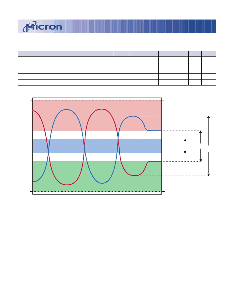
Clock Input Mid-Point Voltage; CK and CK#
Clock Input Voltage Level; CK and CK#
Clock Input Differential Voltage; CK and CK#
Clock Input Differential Voltage; CK and CK#
Clock Input Crossing Point Voltage; CK and CK#
SYMBOL
V
MP
(
DC
)
V
IN
(
DC
)
V
ID
(
DC
)
V
ID
(
AC
)
V
IX
(
AC
)
MIN
1.05
-0.3
0.36
0.7
MAX
1.45
UNITS
V
V
V
V
V
NOTES
6, 9
6
6, 8
8
9
V
DD
Q + 0.3
V
DD
Q + 0.6
V
DD
Q + 0.6
0.5 x V
DD
Q + 0.2
0.5 x V
DD
Q - 0.2
CK#
CK
2.80v
2
3
5
5
Maximum Clock Level
Minimum Clock Level
4
- 0.30v
1.325v
1.525v
1.125v
V
ID
(AC)
V
ID
(DC)
X
X
1
V
MP
(DC)
V
IX
(AC)
NOTE:
1. This provides a minimum of 1.225v to a maximum of 1.425v, and is always half of V
DD
Q.
2. CK and CK# must cross in this region.
3. CK and CK# must meet at least V
ID
(DC) min when static and is centered around V
MP
(DC).
4. CK and CK# must have a minimum 700mv peak to peak swing.
5. CK or CK# may not be more positive than V
DD
Q + 0.5v or more negative than Vss - 0.5v.
6. For AC operation, all DC clock requirements must also be satisfied.
7. Numbers in diagram reflect nominal values.
X
X
FIGURE 27B – SSTL_2 CLOCK INPUT
相關(guān)PDF資料 |
PDF描述 |
|---|---|
| MT46V32M4-1 | DOUBLE DATA RATE DDR SDRAM |
| MT46V32M4TG-75 | DOUBLE DATA RATE DDR SDRAM |
| MT46V32M4TG-75L | DOUBLE DATA RATE DDR SDRAM |
| MT46V32M4TG-75Z | DOUBLE DATA RATE DDR SDRAM |
| MT46V32M4TG-75ZL | DOUBLE DATA RATE DDR SDRAM |
相關(guān)代理商/技術(shù)參數(shù) |
參數(shù)描述 |
|---|---|
| MT46V32M16 | 制造商:Micron Technology Inc 功能描述:32MX16 DDR SDRAM PLASTIC IND TEMP BGA 2.6V DDR - Trays |
| MT46V32M16-5B | 制造商:Micron Technology Inc 功能描述: |
發(fā)布緊急采購,3分鐘左右您將得到回復(fù)。