- 您現(xiàn)在的位置:買賣IC網(wǎng) > PDF目錄371123 > MMBT3416LT3 (ON SEMICONDUCTOR) General Purpose Amplifier(NPN Silicon) PDF資料下載
參數(shù)資料
| 型號(hào): | MMBT3416LT3 |
| 廠商: | ON SEMICONDUCTOR |
| 元件分類: | 小信號(hào)晶體管 |
| 英文描述: | General Purpose Amplifier(NPN Silicon) |
| 中文描述: | 100 mA, 40 V, NPN, Si, SMALL SIGNAL TRANSISTOR, TO-236AB |
| 封裝: | CASE 318-08, TO-236, 3 PIN |
| 文件頁數(shù): | 6/8頁 |
| 文件大?。?/td> | 297K |
| 代理商: | MMBT3416LT3 |
6
Motorola Small–Signal Transistors, FETs and Diodes Device Data
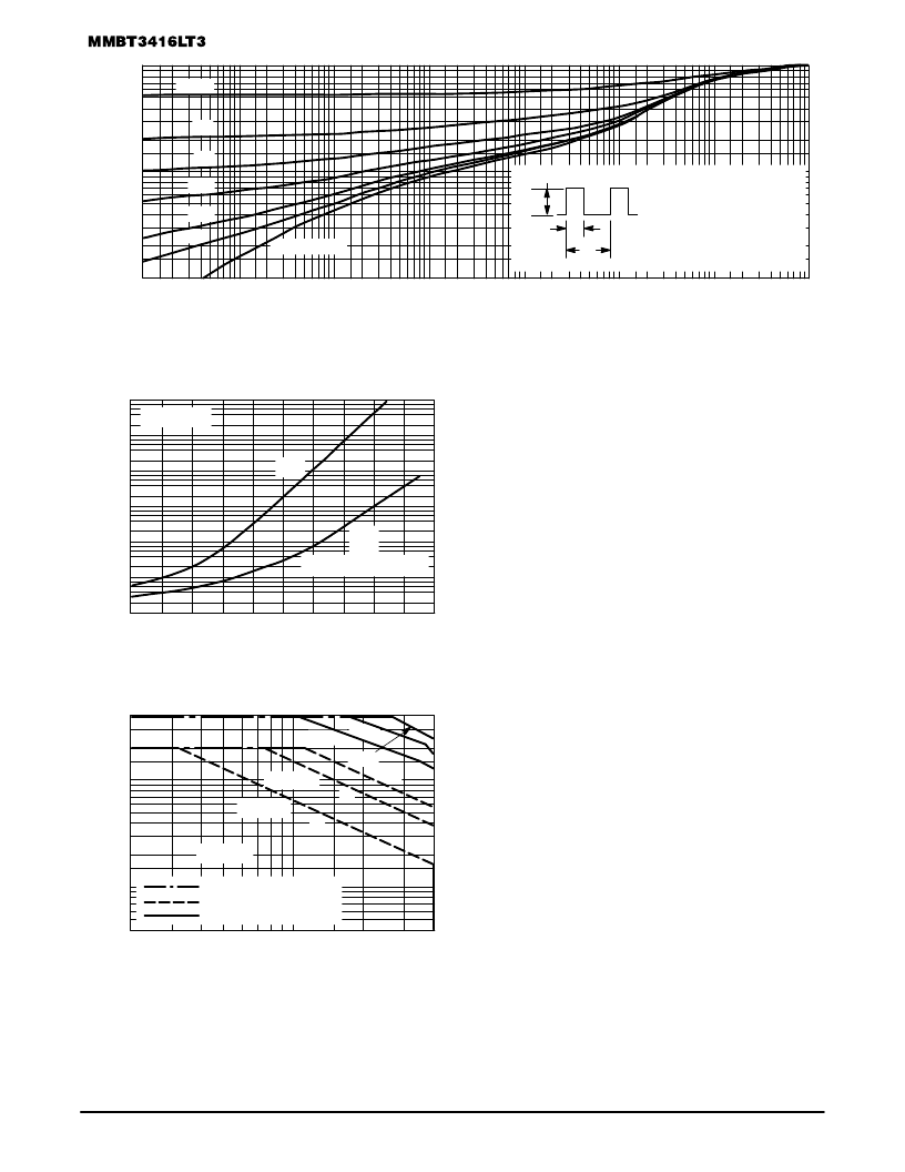
Figure 19. Thermal Response
t, TIME (ms)
1.0
0.7
0.01
r
(
0.01
0.02
0.03
0.05
0.07
0.1
0.2
0.3
0.5
0.02
0.05
0.1
0.2
0.5
1.0
2.0
5.0
10
20
50
100
200
500
1.0 k 2.0 k
5.0 k 10 k
20 k
50 k
100 k
D = 0.5
0.2
0.1
0.05
0.02
0.01
SINGLE PULSE
DUTY CYCLE, D = t1/t2
D CURVES APPLY FOR POWER
PULSE TRAIN SHOWN
READ TIME AT t1 (SEE AN–569)
Z
θ
JA(t) = r(t)
R
θ
JA
TJ(pk) – TA = P(pk) Z
θ
JA(t)
t1
t2
P(pk)
FIGURE 19A
Figure 19A.
TJ, JUNCTION TEMPERATURE (
°
C)
104
–4
0
I
Figure 20.
VCE, COLLECTOR–EMITTER VOLTAGE (VOLTS)
400
2.0
I
DESIGN NOTE: USE OF THERMAL RESPONSE DATA
A train of periodical power pulses can be represented by the model
as shown in Figure 19A. Using the model and the device thermal
response the normalized effective transient thermal resistance of
Figure 19 was calculated for various duty cycles.
To find Z
θ
JA(t), multiply the value obtained from Figure 19 by the
steady state value R
θ
JA.
Example:
The MPS3904 is dissipating 2.0 watts peak under the following
conditions:
t1 = 1.0 ms, t2 = 5.0 ms. (D = 0.2)
Using Figure 19 at a pulse width of 1.0 ms and D = 0.2, the reading of
r(t) is 0.22.
The peak rise in junction temperature is therefore
T = r(t) x P(pk) x R
θ
JA = 0.22 x 2.0 x 200 = 88
°
C.
For more information, see AN–569.
The safe operating area curves indicate IC–VCE limits of the
transistor that must be observed for reliable operation. Collector load
lines for specific circuits must fall below the limits indicated by the
applicable curve.
The data of Figure 20 is based upon TJ(pk) = 150
°
C; TC or TA is
variable depending upon conditions. Pulse curves are valid for duty
cycles to 10% provided TJ(pk)
≤
150
°
C. TJ(pk) may be calculated from
the data in Figure 19. At high case or ambient temperatures, thermal
limitations will reduce the power that can be handled to values less
than the limitations imposed by second breakdown.
10–2
10–1
100
101
102
103
–2
0
0
+20
+40
+60
+80
+100 +120 +140 +160
VCC = 30 Vdc
ICEO
ICBO
AND
ICEX @ VBE(off) = 3.0 Vdc
TA = 25
°
C
CURRENT LIMIT
THERMAL LIMIT
SECOND BREAKDOWN LIMIT
1.0 ms
10
μ
s
TC = 25
°
C
1.0 s
dc
dc
4.0
6.0
10
20
40
60
100
200
4.0
6.0
8.0
10
20
40
TJ = 150
°
C
100
μ
s
相關(guān)PDF資料 |
PDF描述 |
|---|---|
| MMBT5401LT1 | High Voltage Transistor |
| MMBT5401 | PNP SMALL SIGNAL SURFACE MOUNT TRANSISTOR |
| MMBT5401-7 | PNP SMALL SIGNAL SURFACE MOUNT TRANSISTOR |
| MMBT5401W | Mini size of Discrete semiconductor elements |
| MMBT5401 | Mini size of Discrete semiconductor elements |
相關(guān)代理商/技術(shù)參數(shù) |
參數(shù)描述 |
|---|---|
| MMBT3416LT3G | 功能描述:兩極晶體管 - BJT 100mA 60V PNP RoHS:否 制造商:STMicroelectronics 配置: 晶體管極性:PNP 集電極—基極電壓 VCBO: 集電極—發(fā)射極最大電壓 VCEO:- 40 V 發(fā)射極 - 基極電壓 VEBO:- 6 V 集電極—射極飽和電壓: 最大直流電集電極電流: 增益帶寬產(chǎn)品fT: 直流集電極/Base Gain hfe Min:100 A 最大工作溫度: 安裝風(fēng)格:SMD/SMT 封裝 / 箱體:PowerFLAT 2 x 2 |
| MMBT3640 | 功能描述:兩極晶體管 - BJT Switching Transistor PNP RoHS:否 制造商:STMicroelectronics 配置: 晶體管極性:PNP 集電極—基極電壓 VCBO: 集電極—發(fā)射極最大電壓 VCEO:- 40 V 發(fā)射極 - 基極電壓 VEBO:- 6 V 集電極—射極飽和電壓: 最大直流電集電極電流: 增益帶寬產(chǎn)品fT: 直流集電極/Base Gain hfe Min:100 A 最大工作溫度: 安裝風(fēng)格:SMD/SMT 封裝 / 箱體:PowerFLAT 2 x 2 |
| MMBT3640_D87Z | 功能描述:兩極晶體管 - BJT Switching Transistor PNP RoHS:否 制造商:STMicroelectronics 配置: 晶體管極性:PNP 集電極—基極電壓 VCBO: 集電極—發(fā)射極最大電壓 VCEO:- 40 V 發(fā)射極 - 基極電壓 VEBO:- 6 V 集電極—射極飽和電壓: 最大直流電集電極電流: 增益帶寬產(chǎn)品fT: 直流集電極/Base Gain hfe Min:100 A 最大工作溫度: 安裝風(fēng)格:SMD/SMT 封裝 / 箱體:PowerFLAT 2 x 2 |
| MMBT3640_Q | 功能描述:兩極晶體管 - BJT Switching Transistor PNP RoHS:否 制造商:STMicroelectronics 配置: 晶體管極性:PNP 集電極—基極電壓 VCBO: 集電極—發(fā)射極最大電壓 VCEO:- 40 V 發(fā)射極 - 基極電壓 VEBO:- 6 V 集電極—射極飽和電壓: 最大直流電集電極電流: 增益帶寬產(chǎn)品fT: 直流集電極/Base Gain hfe Min:100 A 最大工作溫度: 安裝風(fēng)格:SMD/SMT 封裝 / 箱體:PowerFLAT 2 x 2 |
| MMBT3640-CUT TAPE | 制造商:FAIRCHILD 功能描述:MMBT3640 Series 12 V CE Breakdown .2 A PNP Switching Transistor - SOT-23 |
發(fā)布緊急采購,3分鐘左右您將得到回復(fù)。