- 您現(xiàn)在的位置:買賣IC網(wǎng) > PDF目錄371096 > MCM72FB8ML (Motorola, Inc.) 600000 SYSTEM GATE 1.8 VOLT FPGA - NOT RECOMMENDED for NEW DESIGN PDF資料下載
參數(shù)資料
| 型號: | MCM72FB8ML |
| 廠商: | Motorola, Inc. |
| 元件分類: | FPGA |
| 英文描述: | 600000 SYSTEM GATE 1.8 VOLT FPGA - NOT RECOMMENDED for NEW DESIGN |
| 中文描述: | 256 × 72比特突發(fā)內(nèi)存多芯片模塊 |
| 文件頁數(shù): | 4/20頁 |
| 文件大小: | 252K |
| 代理商: | MCM72FB8ML |
MCM72FB8ML MCM72PB8ML
4
MOTOROLA FAST SRAM
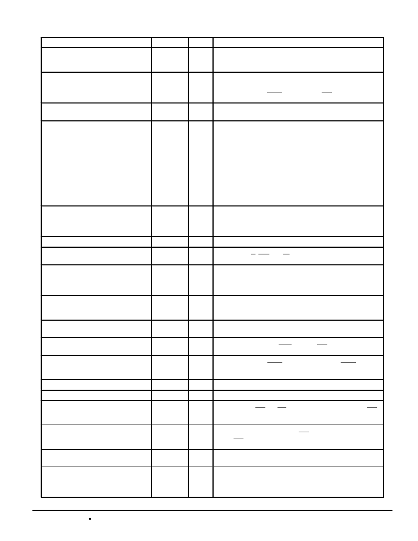
PIN DESCRIPTIONS
Pin Locations
Symbol
Type
Description
E10
ADSC
Input
Synchronous Address Status Controller: Active low, interrupts any
ongoing burst and latches a new external address. Used to initiate
READ, WRITE, or chip deselect cycle.
F10
ADSP
Input
Synchronous Address Status Processor: Active low, interrupts any
ongoing burst and latches a new external address. Used to initiate
READ, WRITE, or chip deselect cycle (exception — chip deselect
does not occur when ADSP is asserted and SE1 is high).
D10
ADV
Input
Synchronous Address Advance: Increments address count in
accordance with counter type selected (linear/interleaved).
(a) R14, T14, T15, U14, U15, V14, V15,
W14, W15
(b) L14, L15, M14, M15, N14, N15, P14,
P15, R15
(c) E14, F14, F15, G14, G15, H14, H15,
J14, J15
(d) A14, A15, B14, B15, C14, C15, D14,
D15, E15
(e) A5, A6, B5, B6, C5, C6, D5, D6, E5
(f) E6, F5, F6, G5, G6, H5, H6, J5, J6
(g) L5, L6, M5, M6, N5, N6, P5, P6, R5
(h) R6, T5, T6, U5, U6, V5, V6, W5, W6
DQx
I/O
Synchronous Data I/O: “x” refers to the byte being read or written
(byte a, b, c, d, e, f, g, h).
U13
FT
Input
Flow–Through Input: This pin must remain in steady state (this
signal is not registered or latched). It must be tied high or low.
Low — flow–through mode.
High — pipeline mode.
B10
G
Input
Asynchronous Output Enable.
R10
K
Input
Clock: This signal registers the address, data in, and all control
signals except G, LBO, and FT.
U7
LBO
Input
Linear Burst Order Input: This pin must remain in steady state (this
signal not registered or latched). It must be tied high or low.
Low — linear burst counter (68K/PowerPC).
High — interleaved burst counter (486/i960/Pentium).
U10, V10
SA1, SA0
Input
Synchronous Address Inputs: These pins must be wired to the two
LSBs of the address bus for proper burst operation. These inputs
are registered and must meet setup and hold times.
A7, A8, A9, A11, A12, A13, B7, B8, B9,
B11, B12, B13, V8, V9, V11, V12
SA2 – SA17
Input
Synchronous Address Inputs: These inputs are registered and must
meet setup and hold times.
L13, K14, K15, J13, J7, K5, K6, L7
(a) (b) (c) (d) (e) (f) (g) (h)
SBx
Input
Synchronous Byte Write Inputs: “x” refers to the byte being written
(byte a, b, c, d, e, f, g, h). SGW overrides SBx.
A10
SE1
Input
Synchronous Chip Enable: Active low to enable chip.
Negated high–blocks ADSP or deselects chip when ADSC is
asserted.
C7
SE2
Input
Synchronous Chip Enable: Active high for depth expansion.
C13
SE3
Input
Synchronous Chip Enable: Active low for depth expansion.
C10
SGW
Input
Synchronous Global Write: This signal writes all bytes regardless of
the status of the SBx and SW signals. If only byte write signals SBx
are being used, tie this pin high.
T10
SW
Input
Synchronous Write: This signal writes only those bytes that have
been selected using the byte write SBx pins. If only byte write
signals SBx are being used, tie this pin low.
D8, D12, E8, E12, F8, F12, G8,
G12, N8, N12, P8, P12, R8, R12, T8, T12
VDD
Supply
Core Power Supply.
C8, C9, C11, C12, D7, D13, E7,
E13, F7, F13, G7, G13, H7, H13,
M7, M13, N7, N13, P7, P13, R7,
R13, T7, T13, U8, U9, U11, U12
VDDQ
Supply
I/O Power Supply.
相關(guān)PDF資料 |
PDF描述 |
|---|---|
| MCM72FB8ML8 | 600,000 SYSTEM GATE 1.8 VOLT FPGA - NOT RECOMMENDED for NEW DESIGN |
| MCR102 | Silicon Controlled Rectifiers |
| MCR103 | Silicon Controlled Rectifiers |
| MCR225FP | Silicon Controlled Rectifiers |
| MCR506 | Silicon Controlled Rectifiers |
相關(guān)代理商/技術(shù)參數(shù) |
參數(shù)描述 |
|---|---|
| MCM72FB8ML7.5 | 制造商:MOTOROLA 制造商全稱:Motorola, Inc 功能描述:256K x 72 Bit Burst RAM Multichip Module |
| MCM72FB8ML7.5R | 制造商:MOTOROLA 制造商全稱:Motorola, Inc 功能描述:256K x 72 Bit Burst RAM Multichip Module |
| MCM72FB8ML8 | 制造商:MOTOROLA 制造商全稱:Motorola, Inc 功能描述:256K x 72 Bit Burst RAM Multichip Module |
| MCM72FB8ML8R | 制造商:MOTOROLA 制造商全稱:Motorola, Inc 功能描述:256K x 72 Bit Burst RAM Multichip Module |
| MCM72JG32 | 制造商:MOTOROLA 制造商全稱:Motorola, Inc 功能描述:256KB and 512KB Pipelined BurstRAM Secondary Cache Module for Pentium |
發(fā)布緊急采購,3分鐘左右您將得到回復(fù)。