- 您現(xiàn)在的位置:買賣IC網(wǎng) > PDF目錄371089 > MCM64E918 (Motorola, Inc.) 8M Bit synchronous late write fast static RAM(8M位同步遲寫快速靜態(tài)RAM) PDF資料下載
參數(shù)資料
| 型號: | MCM64E918 |
| 廠商: | Motorola, Inc. |
| 英文描述: | 8M Bit synchronous late write fast static RAM(8M位同步遲寫快速靜態(tài)RAM) |
| 中文描述: | 晚8分位同步靜態(tài)隨機存儲器寫入速度(800萬位同步遲寫快速靜態(tài)內(nèi)存) |
| 文件頁數(shù): | 1/24頁 |
| 文件大?。?/td> | 503K |
| 代理商: | MCM64E918 |
MCM64E918
MCM64E836
1
MOTOROLA FAST SRAM
Motorola, Inc. 1999
Product Preview
8MB Double Data Rate HSTL I/O
Fast SRAM
The MCM64E918/MCM64E836 are 8M–bit pipelined burst synchronous late
write fast static RAMs designed to provide very high data bandwidth in secondary
cache applications. The MCM64E918 (organized as 512K words by 18 bits wide)
and the MCM64E836 (organized as 256K words by 36 bits wide) are fabricated
in Motorola’s high performance silicon gate MOS technology.
The differential clock (CK) inputs control the timing of read/write operations of
the RAM. At the rising edge of CK, all addresses and burst control inputs are
registered. An internal buffer and special logic enables the memory to accept
write data on the rising or rising and falling edges of the clock, a cycle following
address and control signals. Read data is driven on the rising or rising and falling
edges of the CK clock and is referenced to echo clock (CQ and CQ) outputs.
The MCM64E918/MCM64E836 have HSTL inputs and outputs. The adjust-
able input trip–point (Vref) and output power supply voltage (VDDQ) gives
the system designer greater flexibility in optimizing system performance.
The impedance of the output buffers is programmable, allowing the outputs to
match the impedance of the circuit traces, which reduces signal reflections.
Single 2.5 V
±
5% Power Supply
Single Data Rate (SDR) and Double Data Rate (DDR) Burst Read and
Write
Pin Selectable Linear or Interleaved Burst Order
Four Tick Burst with Automatic Wrap–Around
Differential Clock Inputs
Active High and Active Low Echo Clock Outputs
1.8 V Expanded HSTL — I/O (JEDEC Standard JESD8–6 Class I
Compatible)
1.8 V Expanded HSTL — Compatible Programmable Impedance Output
Drivers
Pipelined (Register to Register) Synchronous Operation
Boundary Scan (JTAG) IEEE 1149.1 Compatible
Stop Clock Functionality Supported
Optional x18 or x36 Organization
MCM64E918/MCM64E836–3.0 = 3.0 ns Clock Cycle Time
MCM64E918/MCM64E836–3.3 = 3.3 ns Clock Cycle Time
MCM64E918/MCM64E836–4.0 = 4.0 ns Clock Cycle Time
MCM64E918/MCM64E836–4.4 = 4.4 ns Clock Cycle Time
MCM64E918/MCM64E836–5.0 = 5.0 ns Clock Cycle Time
9 x 17 (153) Bump, 50 mil (1.27 mm) Pitch, 14 mm x 22 mm Flipped Chip
Plastic Ball Grid Array (PBGA) or Flipped Chip Ceramic Ball Grid Array
(CBGA) Packages
This document contains information on a product under development. Motorola reserves the right to change or discontinue this product without notice.
Order this document
by MC64E918/D
SEMICONDUCTOR TECHNICAL DATA
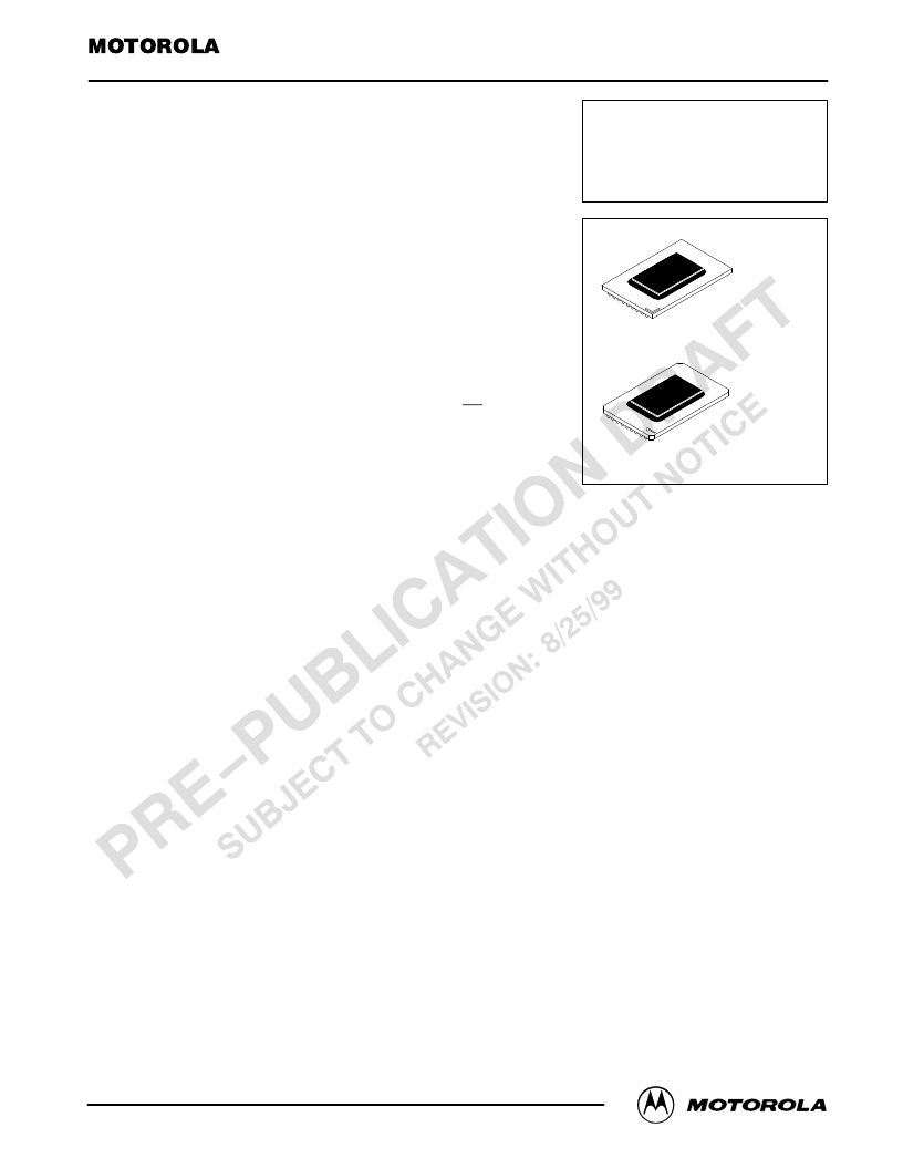
MCM64E918
MCM64E836
FC PACKAGE
FLIPPED CHIP PBGA
CASE 1107A–01
RS PACKAGE
FLIPPED CHIP CBGA
CASE 1107B–01
8/25/99
相關(guān)PDF資料 |
PDF描述 |
|---|---|
| MCM64PC32TSG66 | 256K/512K Pipelined BurstRAM Secondary Cache Module for Pentium |
| MCM64PC64TSG66 | 256K/512K Pipelined BurstRAM Secondary Cache Module for Pentium |
| MCM64PC32T | 256K/512K Pipelined BurstRAM Secondary Cache Module for Pentium |
| MCM6706RJ8 | 32K x 8 Bit Static Random Access Memory |
| MCM6706J6 | Circular Connector; Body Material:Aluminum; Series:PT06; Number of Contacts:41; Connector Shell Size:20; Connecting Termination:Crimp; Circular Shell Style:Straight Plug; Circular Contact Gender:Socket; Insert Arrangement:20-41 |
相關(guān)代理商/技術(shù)參數(shù) |
參數(shù)描述 |
|---|---|
| MCM64PC32 | 制造商:MOTOROLA 制造商全稱:Motorola, Inc 功能描述:256K/512K Pipelined BurstRAM Secondary Cache Module for Pentium |
| MCM64PC32SG66 | 制造商:MOTOROLA 制造商全稱:Motorola, Inc 功能描述:256K/512K Pipelined BurstRAM Secondary Cache Module for Pentium |
| MCM64PC32T | 制造商:MOTOROLA 制造商全稱:Motorola, Inc 功能描述:256K/512K Pipelined BurstRAM Secondary Cache Module for Pentium |
| MCM64PC32TSG66 | 制造商:MOTOROLA 制造商全稱:Motorola, Inc 功能描述:256K/512K Pipelined BurstRAM Secondary Cache Module for Pentium |
| MCM64PC64SG66 | 制造商:MOTOROLA 制造商全稱:Motorola, Inc 功能描述:256K/512K Pipelined BurstRAM Secondary Cache Module for Pentium |
發(fā)布緊急采購,3分鐘左右您將得到回復。