- 您現(xiàn)在的位置:買賣IC網(wǎng) > PDF目錄371003 > MC10E197 (ON SEMICONDUCTOR) DATA SEPARATOR PDF資料下載
參數(shù)資料
| 型號: | MC10E197 |
| 廠商: | ON SEMICONDUCTOR |
| 英文描述: | DATA SEPARATOR |
| 中文描述: | 數(shù)據(jù)分離器 |
| 文件頁數(shù): | 11/16頁 |
| 文件大小: | 217K |
| 代理商: | MC10E197 |

MC10E197
2–11
MOTOROLA
ECLinPS and ECLinPS Lite
DL140 — Rev 4
From Equation 7 the value for the other resistors associated
with the integrator op-amp are set equal to RA:
RlA = RA = 5.11k
Voltage Divider Subsection
The element values for the voltage divider network are
calculated using the relationships presented in Equations 8,
9, and 10 with the constraint that this divider network must
produce a voltage that lies within the range 1.3V + VEE to 2.6V
+ VEE.
Restating Equation 9,
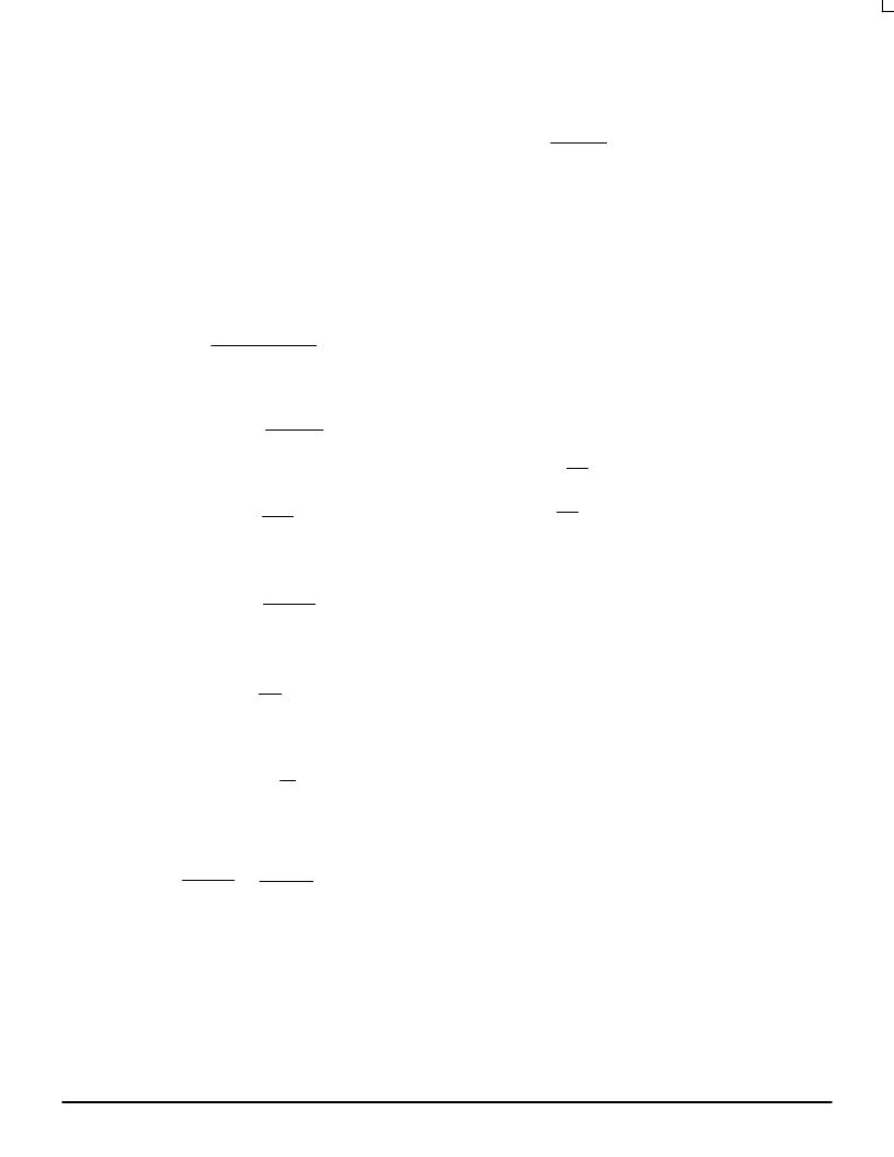
Kd =
Kol
K
φ
* Ko * K1 * Kl
From the root locus analysis Kol is determined to be:
Kol = 1.585 e51
V
mA sec3
From Equation 3
K1 = A1 *
1
CIN
and the gain constant K1 is:
K1 = 8.90 e21
V
mA sec
From Equation 5
Kl = Al *
RA
RlA
and the gain constant Kl is:
Kl = 2.48 e15V
V
Having determined the gain constant Kd , the value of Rv, is
selected such that the constraints Rv > Ro and:
Kd
2
π
p2
=
Ro
Ro + Rv
are fulfilled. The pole position P2 is determined from the root
locus analysis to be:
P2 = – 3.06MHz
Hence, Rv is selected to be:
Rv = 2.15k
and Ro is calculated to be:
Ro = 700
Finally, using Equation 8a:
Cd =
1
Rv Kd
eqt. 8a
the capacitor value, Cd is:
Cd = 98pF
Note that the voltage divider section can be used to set the
gain, but the designer is cautioned to be sure the input
value to VCOIN is within the correct range.
Component Scaling
As mentioned, these design equations were developed for
a data rate of 23 Mbit/sec. If the data rate is different from the
nominal design value the reactive elements must be scaled
accordingly. The following equations are provided to facilitate
scaling and were derived with the assumptions that a 2:7
coding scheme is used and that the RDCLK signal is twice the
frequency of the data clock.
CIN = 278 *46
f
eqt. 11
(pF)
46
f
Cd = 98 *
eqt. 12
(pF)
where f is the RDCLK frequency in MHz.
Example for an 11 Mbit/sec Data Rate
As an example of scaling, assume the given filter and a 2:7
code are used but the data rate is 11Mbit/sec. The dynamic
pole positions, and therefore the bandwidth of the loop filter,
are a function of the data rate. Thus a slower data rate will
force the dynamic poles and the bandwidth to move to a lower
frequency. From Equation 11 the value of CIN is:
CIN = 581pF
and from Equation 12 the value of Cd is:
Cd = 205pF
Thus the element values for the filter are:
Filter Input Subsection:
CIN = 581pF
R1 = 1k
Integrator Subsection:
CA = 0.1
μ
F
RA = 5.11k
RlA = 5.11k
Voltage Divider Subsection:
Cd = 205pF
Rv = 2.15k
Ro = 700k
相關(guān)PDF資料 |
PDF描述 |
|---|---|
| MC10EL32D | Dual 1A Current-Limited, Power-Distribution Switches 8-MSOP-PowerPAD -40 to 85 |
| MC10EL32 | Dual 1A Current-Limited, Power-Distribution Switches 8-SOIC -40 to 85 |
| MC100EL32D | ±2 Divider |
| MC10EL33D | ±4 Divider |
| MC10EL34D | ±2, ±4, ±8 Clock Generation Chip |
相關(guān)代理商/技術(shù)參數(shù) |
參數(shù)描述 |
|---|---|
| MC10E197FN | 制造商:Rochester Electronics LLC 功能描述:- Bulk |
| MC10E211 C14N WAF | 制造商:ON Semiconductor 功能描述: |
| MC10E211FN | 功能描述:時鐘驅(qū)動器及分配 5V ECL 1:6 Diff RoHS:否 制造商:Micrel 乘法/除法因子:1:4 輸出類型:Differential 最大輸出頻率:4.2 GHz 電源電壓-最大: 電源電壓-最小:5 V 最大工作溫度:+ 85 C 封裝 / 箱體:SOIC-8 封裝:Reel |
| MC10E211FNG | 功能描述:時鐘驅(qū)動器及分配 5V ECL 1:6 Diff Clock Driver RoHS:否 制造商:Micrel 乘法/除法因子:1:4 輸出類型:Differential 最大輸出頻率:4.2 GHz 電源電壓-最大: 電源電壓-最小:5 V 最大工作溫度:+ 85 C 封裝 / 箱體:SOIC-8 封裝:Reel |
| MC10E211FNR2 | 功能描述:時鐘驅(qū)動器及分配 5V ECL 1:6 Diff RoHS:否 制造商:Micrel 乘法/除法因子:1:4 輸出類型:Differential 最大輸出頻率:4.2 GHz 電源電壓-最大: 電源電壓-最小:5 V 最大工作溫度:+ 85 C 封裝 / 箱體:SOIC-8 封裝:Reel |
發(fā)布緊急采購,3分鐘左右您將得到回復(fù)。