- 您現(xiàn)在的位置:買賣IC網(wǎng) > PDF目錄45053 > M8803F3Y-90K1T (STMICROELECTRONICS) 1M X 1 FLASH, 27 I/O, PIA-GENERAL PURPOSE, PQCC52 PDF資料下載
參數(shù)資料
| 型號: | M8803F3Y-90K1T |
| 廠商: | STMICROELECTRONICS |
| 元件分類: | 微控制器/微處理器 |
| 英文描述: | 1M X 1 FLASH, 27 I/O, PIA-GENERAL PURPOSE, PQCC52 |
| 封裝: | PLASTIC, LCC-52 |
| 文件頁數(shù): | 37/85頁 |
| 文件大?。?/td> | 601K |
| 代理商: | M8803F3Y-90K1T |
第1頁第2頁第3頁第4頁第5頁第6頁第7頁第8頁第9頁第10頁第11頁第12頁第13頁第14頁第15頁第16頁第17頁第18頁第19頁第20頁第21頁第22頁第23頁第24頁第25頁第26頁第27頁第28頁第29頁第30頁第31頁第32頁第33頁第34頁第35頁第36頁當前第37頁第38頁第39頁第40頁第41頁第42頁第43頁第44頁第45頁第46頁第47頁第48頁第49頁第50頁第51頁第52頁第53頁第54頁第55頁第56頁第57頁第58頁第59頁第60頁第61頁第62頁第63頁第64頁第65頁第66頁第67頁第68頁第69頁第70頁第71頁第72頁第73頁第74頁第75頁第76頁第77頁第78頁第79頁第80頁第81頁第82頁第83頁第84頁第85頁
M88 FAMILY
42/85
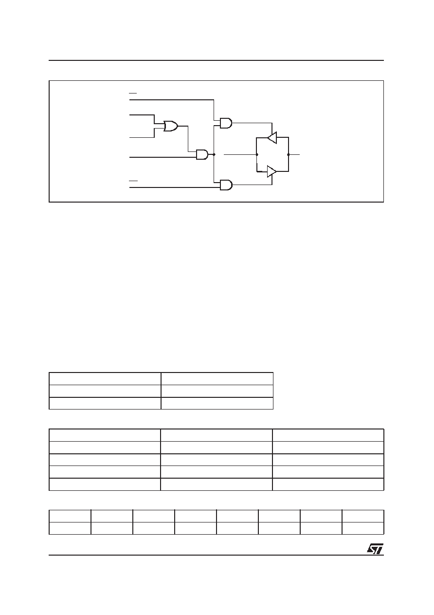
Figu re 28. Peripheral I/O Mode
RD
PSEL0
PSEL1
PSEL
VM REGISTER BIT 7
WR
PA0 - PA7
D0 - D7
DATA BUS
AI02886
The PLD I/O Mode is specified in PSDabel by
declaring the port pins, and then writing an
equation assigning the PLD I/O to a port.
Address Out Mode
For microcontrollers with a multiplexed address/
data bus, Address Out Mode can be used to drive
latched addresses onto the port pins. These port
pins can, in turn, drive external devices. Either the
output enable or the corresponding bits of both the
Direction Register and Control Register must be
set to a ‘1’ for pins to use Address Out Mode. See
Table 24 for the address output pin assignments
on Ports A and B for various MCUs.
For non-multiplexed 8 bit bus mode, address lines
A[7:0] are available to Port B in Address Out
Mode.
Note: Do not drive address lines with Address Out
Mode to an external memory device if it is intended
for the MCU to boot from the external device. The
MCU must first boot from PSD memory so the
Direction and Control register bits can be set.
Address In Mode
For microcontrollers that have more than 16
address lines, the higher addresses can be
connected to Port A, B, C, and D. The address
input can be latched in the Input Macrocell by the
address strobe (ALE/AS). Any input that is
included in the DPLD equations for the PLD’s
Flash, EEPROM, or SRAM is considered to be an
address input.
Table 26. Port Pin Direction Control, Output Enable P.T. Not Defined
Table 27. Port Pin Direction Control, Output Enable P.T. Defined
Table 28. Port Direction Assignment Example
Direction Register Bit
Port Pin Mode
0
Input
1
Output
Direction Register Bit
Outpu t Enable P.T.
Port Pin Mode
0
Input
0
1
Output
1
0
Output
1
Output
Bit 7
Bit 6
Bit 5
Bit 4
Bit 3
Bit 2
Bit 1
Bit 0
00
0
1
相關PDF資料 |
PDF描述 |
|---|---|
| M8813F3Y-90K1T | 1M X 1 FLASH, 27 I/O, PIA-GENERAL PURPOSE, PQCC52 |
| M906-01-125.0000LF | 125 MHz, OTHER CLOCK GENERATOR, CQCC36 |
| M906-01-125.0000LF | 125 MHz, OTHER CLOCK GENERATOR, CQCC36 |
| M906-01-187.5000LF | 187.5 MHz, OTHER CLOCK GENERATOR, CQCC36 |
| M906-01I156.2500 | 156.25 MHz, OTHER CLOCK GENERATOR, CQCC36 |
相關代理商/技術參數(shù) |
參數(shù)描述 |
|---|---|
| M8805/100-007 | 制造商:OTTO Engineering Inc 功能描述:M8805/100-007 |
| M8805/100-009 | 制造商:OTTO Engineering Inc 功能描述:M8805/100-009 |
| M8805/100-010 | 制造商:OTTO Engineering Inc 功能描述:M8805/100-010 |
| M8805/100-015 | 制造商:OTTO Engineering Inc 功能描述:M8805/100-015 |
| M8805/100-016 | 制造商:OTTO Engineering Inc 功能描述:M8805/100-016 |
發(fā)布緊急采購,3分鐘左右您將得到回復。