- 您現(xiàn)在的位置:買賣IC網(wǎng) > PDF目錄384636 > M3773S4B (Mitsubishi Electric Corporation) Single Chip 16 Bits CMOS Microcomputer(16位單片機(jī)) PDF資料下載
參數(shù)資料
| 型號: | M3773S4B |
| 廠商: | Mitsubishi Electric Corporation |
| 英文描述: | Single Chip 16 Bits CMOS Microcomputer(16位單片機(jī)) |
| 中文描述: | 單片微機(jī)16位的CMOS(16位單片機(jī)) |
| 文件頁數(shù): | 7/36頁 |
| 文件大小: | 919K |
| 代理商: | M3773S4B |
第1頁第2頁第3頁第4頁第5頁第6頁當(dāng)前第7頁第8頁第9頁第10頁第11頁第12頁第13頁第14頁第15頁第16頁第17頁第18頁第19頁第20頁第21頁第22頁第23頁第24頁第25頁第26頁第27頁第28頁第29頁第30頁第31頁第32頁第33頁第34頁第35頁第36頁
7
MITSUBISHI MICROCOMPUTERS
M37733S4BFP
16-BIT CMOS MICROCOMPUTER
New product
Pulse output port mode
The pulse motor drive waveform can be output by using plural internal
timer A.
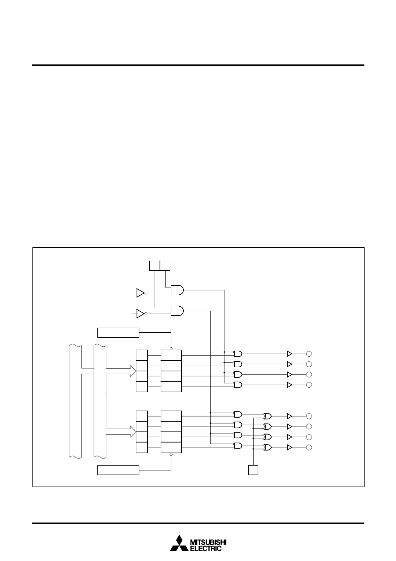
Figure 3 shows a block diagram for pulse output port mode. In the
pulse output port mode, two pairs of four-bit pulse output ports are
used. Whether using pulse output port or not can be selected by
waveform output selection bit (bit 0, bit 1) of waveform output mode
register (62
16
address) shown in Figure 4. When bit 0 of waveform
output selection bit is set to “1”, RTP1
0
, RTP1
1
, RTP1
2
, and RTP1
3
are used as pulse output ports, and when bit 1 of waveform output
selection bit is set to “1”, RTP0
0
, RTP0
1
, RTP0
2
, and RTP0
3
are
used as pulse output ports. When bits 1 and 0 of waveform output
selection bit are set to “1”, RTP1
0
, RTP1
1
, RTP1
2
, and RTP1
3
, and
RTP0
0
, RTP0
1
, RTP0
2,
and RTP0
3
are used as pulse output ports.
The ports not used as pulse output ports can be used as normal
parallel ports, timer input/output or key input interruput input.
In the pulse output port mode, set timers A0 and A2 to timer mode as
timers A0 and A2 are used. Figure 5 shows the bit configuration of
timer A0, A2 mode registers in pulse output port mode.
Data can be set in each bit of the pulse output data register
corresponding to four ports selected as pulse output ports. Figure 6
shows the bit configuration of the pulse output data register. The
contents of the pulse output data register 1 (low-order four bits of
1C
16
address) corresponding to RTP1
0
, RTP1
1
, RTP1
2
, and RTP1
3
is output to the ports each time the counter of timer A2 becomes
0000
16
. The contents of the pulse output data register 0 (low-order
four bits of 1D
16
address) corresponding to RTP0
0
, RTP0
1
, RTP0
2
,
and RTP0
3
is output to the ports each time the counter of timer A0
becomes 0000
16
.
Figure 7 shows example of waveforms in pulse output port mode.
When “0” is written to a specified bit of the pulse output data register,
“L” level is output to the corresponding pulse output port when the
counter of corresponding timer becomes 0000
16
, and when “1” is
written, “H” level is output to the pulse output port.
Pulse width modulation can be applied to each pulse output port.
Since pulse width modulation involves the use of timers A1 and A3,
activate these timers in pulse width modulation mode.
Fig. 3 Block diagram for pulse output port mode
Timer A2
Pulse width modulation output
by timer A3
Pulse width modulation output
by timer A1
D
3
D
2
D
1
D
0
D
D
D
D
Q
Q
Q
Q
T
D
11
D
10
D
9
D
8
D
D
D
D
Q
Q
Q
Q
T
Timer A0
Pulse output data
register 0 (1D
16
address)
Pulse output data
register 1 (1C
16
address)
Pulse width modulation selection bit
(Bit 4, 5 of 62
16
address)
RTP1
3
(P5
7
)
RTP1
2
(P5
6
)
RTP1
1
(
P5
5
)
RTP1
0
(P5
4
)
RTP0
3
(P5
3
)
RTP0
2
(P5
2
)
RTP0
1
(P5
1
)
RTP0
0
(P5
0
)
Polarity selection bit
(Bit 3 of 62
16
address)
4
5
D
D
相關(guān)PDF資料 |
PDF描述 |
|---|---|
| M3773S4L | Single Chip 16 Bits CMOS Microcomputer(16位單片機(jī)) |
| M37751 | 16-Bit Single-Chip Microcomputer(16位單片微控制器) |
| M37753M6C | Single Chip 16 Bits CMOS Microcomputer(16位單片機(jī)) |
| M37753M8C | Single Chip 16 Bits CMOS Microcomputer(16位單片機(jī)) |
| M37754M6C | Single Chip 16 Bits CMOS Microcomputer(16位單片機(jī)) |
相關(guān)代理商/技術(shù)參數(shù) |
參數(shù)描述 |
|---|---|
| M37753FFCFP | 制造商:MITSUBISHI 制造商全稱:Mitsubishi Electric Semiconductor 功能描述:SINGLE CHIP 16 BIT CMOS MICROCOMPUTER FLASH MEMORY VERSION |
| M37753FFCHP | 制造商:MITSUBISHI 制造商全稱:Mitsubishi Electric Semiconductor 功能描述:SINGLE CHIP 16 BIT CMOS MICROCOMPUTER FLASH MEMORY VERSION |
| M37753M6C-XXXFP | 制造商:RENESAS 制造商全稱:Renesas Technology Corp 功能描述:SINGLE-CHIP 16-BIT CMOS MICROCOMPUTER |
| M37753M6C-XXXHP | 制造商:RENESAS 制造商全稱:Renesas Technology Corp 功能描述:SINGLE-CHIP 16-BIT CMOS MICROCOMPUTER |
| M37753M8C-XXXFP | 制造商:RENESAS 制造商全稱:Renesas Technology Corp 功能描述:SINGLE-CHIP 16-BIT CMOS MICROCOMPUTER |
發(fā)布緊急采購,3分鐘左右您將得到回復(fù)。