- 您現(xiàn)在的位置:買(mǎi)賣(mài)IC網(wǎng) > PDF目錄384636 > M3773S4B (Mitsubishi Electric Corporation) Single Chip 16 Bits CMOS Microcomputer(16位單片機(jī)) PDF資料下載
參數(shù)資料
| 型號(hào): | M3773S4B |
| 廠商: | Mitsubishi Electric Corporation |
| 英文描述: | Single Chip 16 Bits CMOS Microcomputer(16位單片機(jī)) |
| 中文描述: | 單片微機(jī)16位的CMOS(16位單片機(jī)) |
| 文件頁(yè)數(shù): | 4/36頁(yè) |
| 文件大小: | 919K |
| 代理商: | M3773S4B |
第1頁(yè)第2頁(yè)第3頁(yè)當(dāng)前第4頁(yè)第5頁(yè)第6頁(yè)第7頁(yè)第8頁(yè)第9頁(yè)第10頁(yè)第11頁(yè)第12頁(yè)第13頁(yè)第14頁(yè)第15頁(yè)第16頁(yè)第17頁(yè)第18頁(yè)第19頁(yè)第20頁(yè)第21頁(yè)第22頁(yè)第23頁(yè)第24頁(yè)第25頁(yè)第26頁(yè)第27頁(yè)第28頁(yè)第29頁(yè)第30頁(yè)第31頁(yè)第32頁(yè)第33頁(yè)第34頁(yè)第35頁(yè)第36頁(yè)
4
MITSUBISHI MICROCOMPUTERS
M37733S4BFP
16-BIT CMOS MICROCOMPUTER
New product
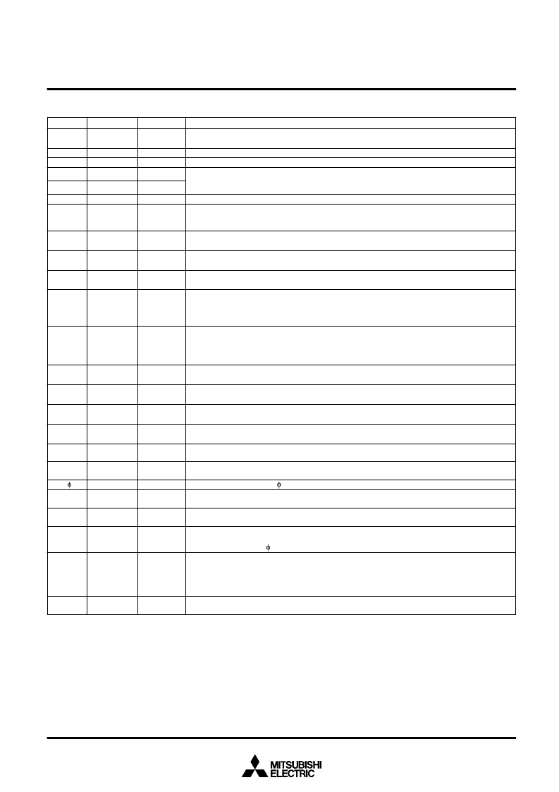
PIN DESCRIPTION
Pin
Vcc,
Power source
Vss
CNVss
CNVss input
RESET
Reset input
X
IN
Clock input
Input
X
OUT
_
E
BYTE
Clock output
Enable output
Bus width
selection input
Output
Output
Input
Name
Input/Output
Functions
Apply 5 V ± 10 % to Vcc and 0 V to Vss.
Input
Input
Connect to Vcc.
When “L” level is applied to this pin, the microcomputer enters the reset state.
These are pins of main-clock generating circuit. Connect a ceramic resonator or a quartz-crystal
oscillator between X
IN
and X
OUT
. When an external clock is used, the clock source should be
connected to the X
IN
pin, and the X
OUT
pin should be left open.
When output level of
E
signal is “L”, data/instruction read or data write is performed.
This pin determines whether the external data bus has an 8-bit width or a 16-bit width.
The data bus has a 16-bit width when “L” signal is input and an 8-bit width when “H” signal
is input.
Power source input pin for the A-D converter. Externally connect AVcc to Vcc and AVss to Vss.
AVcc,
AVss
V
REF
Analog power
source input
Reference
voltage input
Address (low-
order) output
Input
This is reference voltage input pin for the A-D converter.
P0
0
/A
0
–
P0
7
/A
7
P1
0
/A
8
/D
8
–
Address (middle
P1
7
/A
15
/D
15
-order)
output/data
(high-order) I/O
P2
0
/A
16
/D
0
– Address (high-
P2
7
/A
23
/D
7
order)
output/data
(low-order) I/O
_
P3
0
/R/
W
Read/Write
output
___
P3
1
/
BHE
Byte high
enable output
P3
2
/ALE
Address latch
enable output
P3
3
/
HLDA
Hold acknow-
ledge output
HOLD
Hold request
input
RDY
Ready input
Output
Address (A
0
– A
7
) is output.
I/O
When the BYTE pin is set
to
“L”
and
external data bus has a 16-bit width, high-order data
(D
8
– D
15
) is input/output or an address (A
8
– A
15
) is output. When the BYTE pin is “H” and an
external data bus has an 8-bit width, only address (A
8
– A
15
) is output.
I/O
Low-order data (D
0
– D
7
) is input/output or an address (A
16
– A
23
) is output.
Output
“H” indicates the read status and “L” indicates the write status.
Output
“L” is output when an odd-numbered address is accessed.
Output
This is used to retrieve only the address from address and data multiplex signal.
Output
This outputs “L” level when the microcomputer enters hold state after a hold request is accepted.
Input
This is an input pin for
HOLD
request signal. The microcomputer enters into hold state while this
signal is “L”.
This is an input pin for
RDY
signal. The microcomputer enters into ready state while this signal is
“L”.
This pin outputs the clock
These pins become a 5-bit I/O port. An I/O direction register is available so that each pin can be
programmed for input or output. These ports are in the input mode when reset.
In addition to having the same functions as port P4, these pins also function as I/O pins for timers
A0 to A3 and input pins for key input interrupt input (
KI
0
–
KI
3
).
In addition to having the same functions as port P4, these pins also function as I/O pins for timer
A4, input pins for external interrupt input (
INT
0
–
INT
2
) and input pins for timers B0 to B2. P6
7
also
functions as sub-clock
In addition to having the same functions as port P4, these pins function as input pins for A-D
converter. P7
2
to P7
5
also function as I/O pins for UART2. Additionally, P7
6
and P7
7
have the
function as the output pin (X
COUT
) and the input pin (X
CIN
) of the sub-clock (32 kHz) oscillation
circuit, respectively. When P7
6
and P7
7
are used as the X
COUT
and X
CIN
pins, connect a resonator
or an oscillator between the both.
In addition to having the same functions as port P4, these pins also function as I/O pins for UART
0 and UART 1.
Input
P4
2
/
P4
3
– P4
7
1
Clock output
I/O port P4
Output
I/O
1
.
P5
0
– P5
7
I/O port P5
I/O
P6
0
– P6
7
I/O port P6
I/O
SUB
output pin.
P7
0
– P7
7
I/O port P7
I/O
P8
0
– P8
7
I/O port P8
I/O
相關(guān)PDF資料 |
PDF描述 |
|---|---|
| M3773S4L | Single Chip 16 Bits CMOS Microcomputer(16位單片機(jī)) |
| M37751 | 16-Bit Single-Chip Microcomputer(16位單片微控制器) |
| M37753M6C | Single Chip 16 Bits CMOS Microcomputer(16位單片機(jī)) |
| M37753M8C | Single Chip 16 Bits CMOS Microcomputer(16位單片機(jī)) |
| M37754M6C | Single Chip 16 Bits CMOS Microcomputer(16位單片機(jī)) |
相關(guān)代理商/技術(shù)參數(shù) |
參數(shù)描述 |
|---|---|
| M37753FFCFP | 制造商:MITSUBISHI 制造商全稱(chēng):Mitsubishi Electric Semiconductor 功能描述:SINGLE CHIP 16 BIT CMOS MICROCOMPUTER FLASH MEMORY VERSION |
| M37753FFCHP | 制造商:MITSUBISHI 制造商全稱(chēng):Mitsubishi Electric Semiconductor 功能描述:SINGLE CHIP 16 BIT CMOS MICROCOMPUTER FLASH MEMORY VERSION |
| M37753M6C-XXXFP | 制造商:RENESAS 制造商全稱(chēng):Renesas Technology Corp 功能描述:SINGLE-CHIP 16-BIT CMOS MICROCOMPUTER |
| M37753M6C-XXXHP | 制造商:RENESAS 制造商全稱(chēng):Renesas Technology Corp 功能描述:SINGLE-CHIP 16-BIT CMOS MICROCOMPUTER |
| M37753M8C-XXXFP | 制造商:RENESAS 制造商全稱(chēng):Renesas Technology Corp 功能描述:SINGLE-CHIP 16-BIT CMOS MICROCOMPUTER |
發(fā)布緊急采購(gòu),3分鐘左右您將得到回復(fù)。