- 您現(xiàn)在的位置:買賣IC網(wǎng) > PDF目錄98006 > M37735MHBXXXFP 16-BIT, MROM, 25 MHz, MICROCONTROLLER, PQFP80 PDF資料下載
參數(shù)資料
| 型號: | M37735MHBXXXFP |
| 元件分類: | 微控制器/微處理器 |
| 英文描述: | 16-BIT, MROM, 25 MHz, MICROCONTROLLER, PQFP80 |
| 封裝: | 14 X 20 MM, PLASTIC, QFP-80 |
| 文件頁數(shù): | 36/90頁 |
| 文件大小: | 1575K |
| 代理商: | M37735MHBXXXFP |
第1頁第2頁第3頁第4頁第5頁第6頁第7頁第8頁第9頁第10頁第11頁第12頁第13頁第14頁第15頁第16頁第17頁第18頁第19頁第20頁第21頁第22頁第23頁第24頁第25頁第26頁第27頁第28頁第29頁第30頁第31頁第32頁第33頁第34頁第35頁當前第36頁第37頁第38頁第39頁第40頁第41頁第42頁第43頁第44頁第45頁第46頁第47頁第48頁第49頁第50頁第51頁第52頁第53頁第54頁第55頁第56頁第57頁第58頁第59頁第60頁第61頁第62頁第63頁第64頁第65頁第66頁第67頁第68頁第69頁第70頁第71頁第72頁第73頁第74頁第75頁第76頁第77頁第78頁第79頁第80頁第81頁第82頁第83頁第84頁第85頁第86頁第87頁第88頁第89頁第90頁

41
MITSUBISHI MICROCOMPUTERS
M37735MHBXXXFP
SINGLE-CHIP 16-BIT CMOS MICROCOMPUTER
PRELIMINAR
Y
Notice:
This
is not
a final
specification.
Some
parametric
limits
are
subject
to change.
A-D CONVERTER
The A-D converter is an 10-bit successive approximation converter.
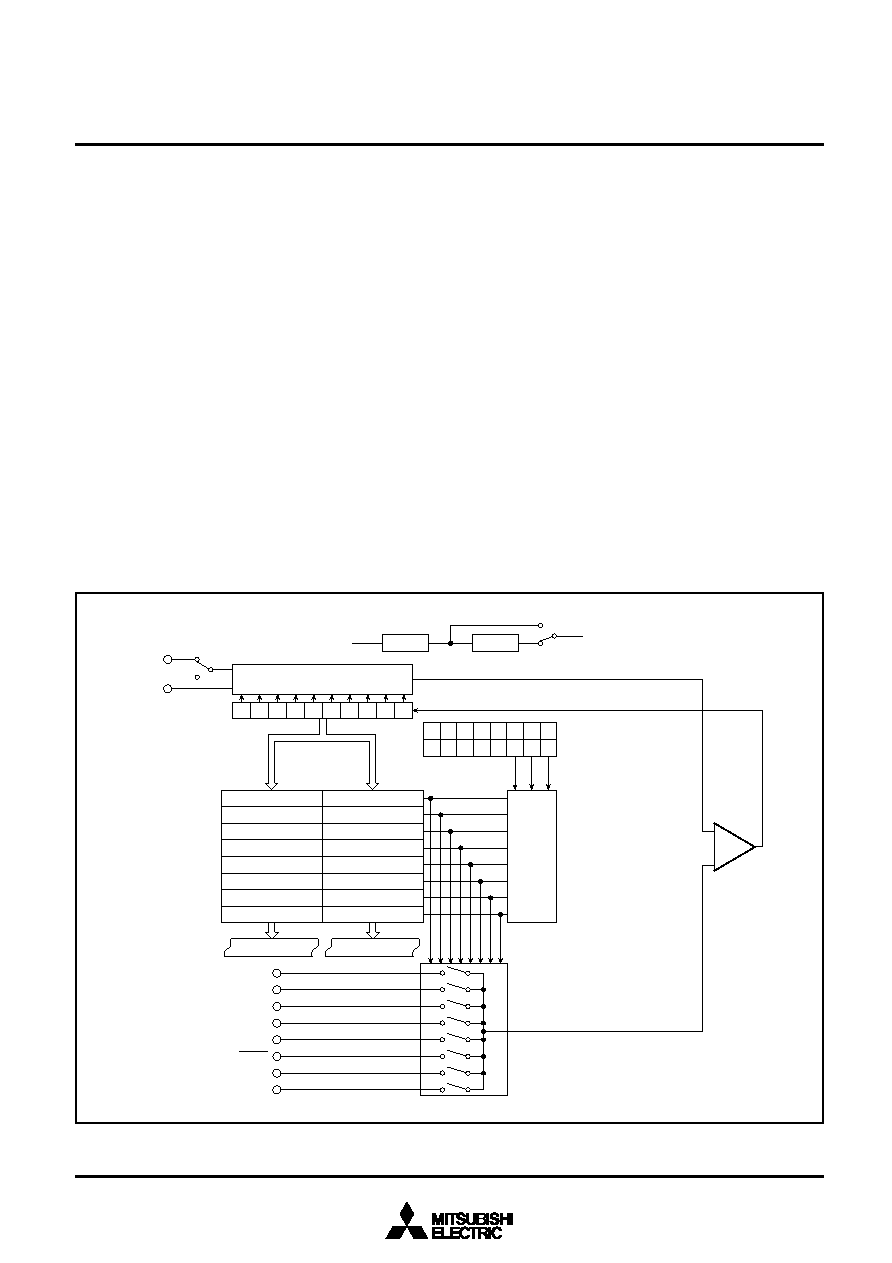
Figure 49 shows a block diagram of the A-D converter and Figure 50
shows the configuration of the A-D control register 0 (address 1E16)
and A-D control register 1 (address 1F16).
The frequency of the A-D converter operating clock
φ AD is selected
by bit 7 of the A-D control register 0. When bit 7 is “0”,
φ AD is the
clock frequency divided by 4. That is,
φ AD = f2/4. When bit 7 is “1”,
φ AD is the clock frequency divided by 2 and φ AD = f2/2.
The
φ AD during A-D conversion must be 250 kHz or more because
the comparator uses a capacity coupling amplifier.
Bit 3 of A-D control register 1 is used to select whether to use the
conversion result as 10 bits or as 8 bits. The conversion result is
used as 10 bits when bit 3 is “1” and as 8 bits when bit 3 is “0”.
When the conversion result is used as 10 bits, the low-order 8 bits of
the conversion result is stored in the even address of the
corresponding A-D register and the high-order two bits are stored in
bits 0 and 1 of the odd address of the corresponding A-D register.
Bits 2 to 7 of the A-D register odd address return “0000002” when
read.
When the conversion result is used as 8 bits, the high-order 8 bits of
the 10-bit A-D conversion are stored in even address of the
corresponding A-D register. In this case, the A-D register odd address
returns “0016” when read.
The operating mode is selected by bits 3 and 4 of A-D control register
0. The available operating modes are one-shot, repeat, single sweep,
repeat sweep.
Whether to connect the reference voltage input pin (VREF) with the
ladder network or not depends on bit 5 of the A-D control register 1.
The VREF pin is connected when bit 5 is “0” and is disconnected
when bit 5 is “1” (High impedance state). When A-D conversion is
not performed, current from the VREF pin to the ladder network can
be cut off by disconnecting ladder network from the VREF pin.
Before starting A-D conversion, wait for 1
s or more after clearing
bit 5 to “0”.
The bit of the port direction register corresponding to the analog input
pin to be used must be “0” (input mode) because the analog input pin
is also used as port P7.
Note that when using the sub-clock (XCIN - XCOUT) or UART2, the
analog pins shared with those functions cannot be used.
The operation of each mode is described below.
The interrupt vector and the interrupt control register are common to
the A-D conversion interrupt and UART2 transmit/receive interrupt.
It is switched by a selection of UART2 function as shown in Figure
37’s note.
Fig. 49 A-D converter block diagram
Data bus (odd)
Data bus (even)
Selector
AN0
AN1
AN2
AN3
AN4
AN5/ADTRG
AN6
AN7
Ladder network
Vref
Successive approximation register
Address
1/2
f2
1/2
A-D register 0 (2116)
A-D register 1 (2316)
A-D register 2 (2516)
A-D register 3 (2716)
A-D register 4 (2916)
A-D register 5 (2B16)
A-D register 6 (2D16)
A-D register 7 (2F16)
A-D register 0 (2016)
A-D register 1 (2216)
A-D register 2 (2416)
A-D register 3 (2616)
A-D register 4 (2816)
A-D register 5 (2A16)
A-D register 6 (2C16)
A-D register 7 (2E16)
Decoder
Comparator
A-D control register 1 (1F16)
A-D control register 0 (1E16)
VREF
AVSS
VREF connect selection
φ AD selection
φ AD
相關PDF資料 |
PDF描述 |
|---|---|
| M37735MHLXXXHP | 16-BIT, MROM, 12 MHz, MICROCONTROLLER, PQFP80 |
| M37736EHLXXXHP | 16-BIT, OTPROM, 12 MHz, MICROCONTROLLER, PQFP100 |
| M37736M4BXXXGP | 16-BIT, MROM, MICROCONTROLLER, PQFP100 |
| M37751M6C-XXXFP | 16-BIT, MROM, 40 MHz, MICROCONTROLLER, PQFP80 |
| M37753M6C-XXXFP | 16-BIT, MROM, 40 MHz, MICROCONTROLLER, PQFP80 |
相關代理商/技術參數(shù) |
參數(shù)描述 |
|---|---|
| M37735MHL | 制造商:MITSUBISHI 制造商全稱:Mitsubishi Electric Semiconductor 功能描述:SINGLE-CHIP 16-BIT CMOS MICROCOMPUTER |
| M37735MHL-143HP | 制造商:MITSUBISHI 制造商全稱:Mitsubishi Electric Semiconductor 功能描述:PROM VERSION OF M37735MHLXXXHP |
| M37735MHLXXXHP | 制造商:RENESAS 制造商全稱:Renesas Technology Corp 功能描述:SINGLE-CHIP 16-BIT CMOS MICROCOMPUTER |
| M37735S4BFP | 制造商:RENESAS 制造商全稱:Renesas Technology Corp 功能描述:16-BIT CMOS MICROCOMPUTER |
| M37735S4LHP | 制造商:RENESAS 制造商全稱:Renesas Technology Corp 功能描述:16-BIT CMOS MICROCOMPUTER |
發(fā)布緊急采購,3分鐘左右您將得到回復。