- 您現(xiàn)在的位置:買賣IC網(wǎng) > PDF目錄98006 > M37510E6-FS 8-BIT, UVPROM, 8 MHz, MICROCONTROLLER, CQCC160 PDF資料下載
參數(shù)資料
| 型號(hào): | M37510E6-FS |
| 元件分類: | 微控制器/微處理器 |
| 英文描述: | 8-BIT, UVPROM, 8 MHz, MICROCONTROLLER, CQCC160 |
| 封裝: | WINDOWED, GLASS SEALED, LCC-160 |
| 文件頁(yè)數(shù): | 43/43頁(yè) |
| 文件大?。?/td> | 614K |
| 代理商: | M37510E6-FS |
第1頁(yè)第2頁(yè)第3頁(yè)第4頁(yè)第5頁(yè)第6頁(yè)第7頁(yè)第8頁(yè)第9頁(yè)第10頁(yè)第11頁(yè)第12頁(yè)第13頁(yè)第14頁(yè)第15頁(yè)第16頁(yè)第17頁(yè)第18頁(yè)第19頁(yè)第20頁(yè)第21頁(yè)第22頁(yè)第23頁(yè)第24頁(yè)第25頁(yè)第26頁(yè)第27頁(yè)第28頁(yè)第29頁(yè)第30頁(yè)第31頁(yè)第32頁(yè)第33頁(yè)第34頁(yè)第35頁(yè)第36頁(yè)第37頁(yè)第38頁(yè)第39頁(yè)第40頁(yè)第41頁(yè)第42頁(yè)當(dāng)前第43頁(yè)

9
7510 Group
SINGLE-CHIP 8-BIT CMOS MICROCOMPUTER
MITSUBISHI MICROCOMPUTERS
Timer X function I/O
Timer Y function I/O
Port P5
Common
Segment
P00–P07
P10–P17
P20–P27
I/O PORTS
Direction Registers
The 7510 group has 41 programmable I/O pins arranged in six I/O
ports (ports P0 to P5). The I/O ports have direction registers which
determine the input/output direction of each individual pin. Each
bit in a direction register corresponds to one pin, each pin can be
set to be input or output.
When “0” is written to the bit corresponding to a pin, that pin be-
comes an input pin. When “1” is written to that bit, that pin
becomes an output pin.
If data is read from a pin which is set for output, the value of the
port output latch is read, not the value of the pin itself. Pins set to
input are floating and can read the value of the pin itself. If a pin
set to input is written to, only the port output latch is written to and
the pin remains floating.
Port Pull-up Control Registers
The 7510 group is equipped with internal pull-ups that can be en-
abled by software. Each I/O port of ports P0–P5 has an port Pi (i=
0 to 5) pull-up control register (addresses 000C16 to 001116). Each
bit of the pull-up control register controls a corresponding bit of the
port. The value written to each individual bit determines whether
the pull-up of the corresponding pin is either enabled or disabled.
When “0” is written to the pull-up control register, the pull up on the
pin is disabled. When “1” is written to the pull-up control register,
the pull-up on the pin is enabled.
After reset, all the pull-up control registers are initialized to “0016”,
disabling all the internal pull-ups.
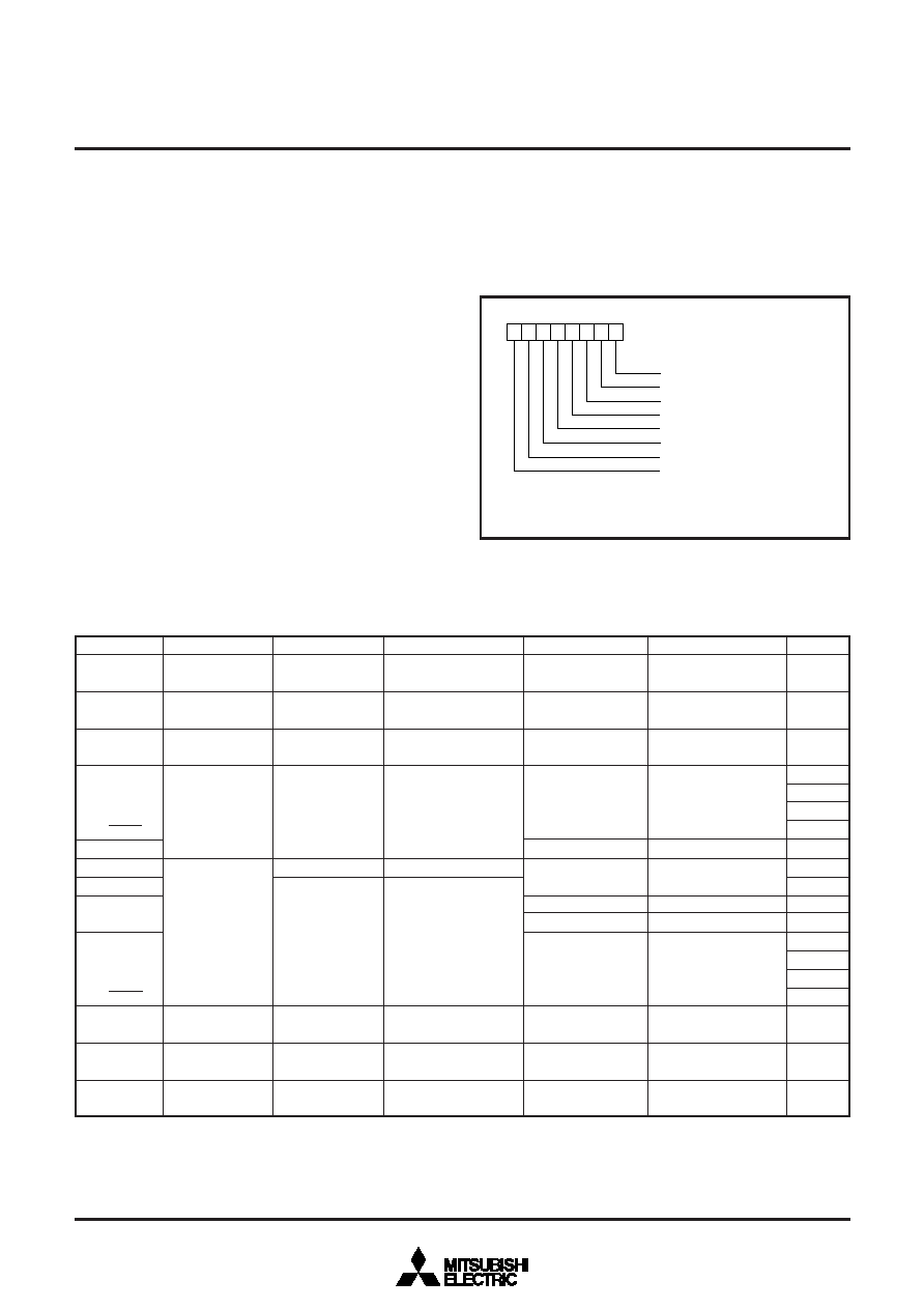
Fig. 4 Structure of port Pi pull-up control register
Pin
Name
Input/Output
I/O Format
Port P0
Port P1
Port P2
Non-Port Function
Related SFRs
Port P3
Port P4
Input/output,
individual bits
Input
Input/output,
individual bits
Input/output,
individual bits
Output
CMOS compatible
input level
CMOS 3-state output
CMOS compatible input level
CMOS compatible
input level
CMOS 3-state output
CMOS compatible input level
CMOS 3-state output
LCD common output
LCD segment output
Key-on wake up
interrupt input
Serial I/O2
function I/O
External interrupt
input
Serial I/O1
function I/O
Sub-clock generat-
ing circuit I/O
P30/RXD2,
P31/TXD2,
P32/ SCLK2,
P33/SRDY2
P34–P37
P40/INT0
P41/INT1
P42/CNTR0,
P43/CNTR1
P44/RXD1,
P45/TXD1,
P46/ SCLK1,
P47/SRDY1
P50/XCOUT,
P51/XCIN
COM0–
COM15
SEG0–
SEG79
CPU mode register
LCD mode register
Interrupt control
register 2
Serial I/O2 control
register
Serial I/O2 status register
UART control register 2
Timer X mode register
Timer Y mode register
Serial I/O1 control
register
Serial I/O1 status register
UART1 control register
Ref. No.
(1)
(2)
(3)
(4)
(5)
(6)
(1)
(7)
(8)
(9)
(8)
(3)
(4)
(5)
(6)
(1)
Notes 1: For details of how to use double-function ports as function I/O ports, refer to the applicable sections.
2: Make sure that the input level at each pin is either 0 V or VCC during execution of the STP instruction.
When an input level is at an intermediate potential, a current will flow from VCC to VSS through the input-stage gate.
Input/output,
individual bits
Input/output,
individual bits
Input/output,
individual bits
CMOS compatible input level
CMOS 3-state output
CMOS compatible input level
CMOS 3-state output
CMOS compatible input level
CMOS 3-state output
b7
Port Pi pull-up control register
(PULLPi : addresses 000C16 to 001116)
Pi0 pull-up
Pi1 pull-up
Pi2 pull-up
Pi3 pull-up
Pi4 pull-up
Pi5 pull-up
Pi6 pull-up
Pi7 pull-up
b0
0 : Disabled
1 : Enabled
i = 0 to 5
相關(guān)PDF資料 |
PDF描述 |
|---|---|
| M37510E6-XXXFP | 8-BIT, OTPROM, 4 MHz, MICROCONTROLLER, PQFP176 |
| M37516M6H-XXXKP | 8-BIT, MROM, 4 MHz, MICROCONTROLLER, PQFP44 |
| M37516M4H-XXXKP | 8-BIT, MROM, 4 MHz, MICROCONTROLLER, PQFP44 |
| M37516M6H-XXXKP | 8-BIT, MROM, 4 MHz, MICROCONTROLLER, PQFP44 |
| M37532E8FP | 8-BIT, OTPROM, 6 MHz, MICROCONTROLLER, PDSO36 |
相關(guān)代理商/技術(shù)參數(shù) |
參數(shù)描述 |
|---|---|
| M37510E7156FP | 制造商:MITSUBISHI 制造商全稱:Mitsubishi Electric Semiconductor 功能描述:SINGLE-CHIP 8-BIT CMOS MICROCOMPUTER |
| M37510E8156FP | 制造商:MITSUBISHI 制造商全稱:Mitsubishi Electric Semiconductor 功能描述:SINGLE-CHIP 8-BIT CMOS MICROCOMPUTER |
| M37510M1156FP | 制造商:MITSUBISHI 制造商全稱:Mitsubishi Electric Semiconductor 功能描述:SINGLE-CHIP 8-BIT CMOS MICROCOMPUTER |
| M37510M2156FP | 制造商:MITSUBISHI 制造商全稱:Mitsubishi Electric Semiconductor 功能描述:SINGLE-CHIP 8-BIT CMOS MICROCOMPUTER |
| M37510M3156FP | 制造商:MITSUBISHI 制造商全稱:Mitsubishi Electric Semiconductor 功能描述:SINGLE-CHIP 8-BIT CMOS MICROCOMPUTER |
發(fā)布緊急采購(gòu),3分鐘左右您將得到回復(fù)。