- 您現在的位置:買賣IC網 > PDF目錄370837 > M32000D3FP (Mitsubishi Electric Corporation) SINGLE-CHIP 32-BIT CMOS MICROCOMPUTER PDF資料下載
參數資料
| 型號: | M32000D3FP |
| 廠商: | Mitsubishi Electric Corporation |
| 英文描述: | SINGLE-CHIP 32-BIT CMOS MICROCOMPUTER |
| 中文描述: | 單芯片32位CMOS微機 |
| 文件頁數: | 20/45頁 |
| 文件大小: | 565K |
| 代理商: | M32000D3FP |
第1頁第2頁第3頁第4頁第5頁第6頁第7頁第8頁第9頁第10頁第11頁第12頁第13頁第14頁第15頁第16頁第17頁第18頁第19頁當前第20頁第21頁第22頁第23頁第24頁第25頁第26頁第27頁第28頁第29頁第30頁第31頁第32頁第33頁第34頁第35頁第36頁第37頁第38頁第39頁第40頁第41頁第42頁第43頁第44頁第45頁
SINGLE-CHIP 32-BIT CMOS MICROCOMPUTER
MITSUBISHI MICROCOMPUTERS
M32000D3FP
20
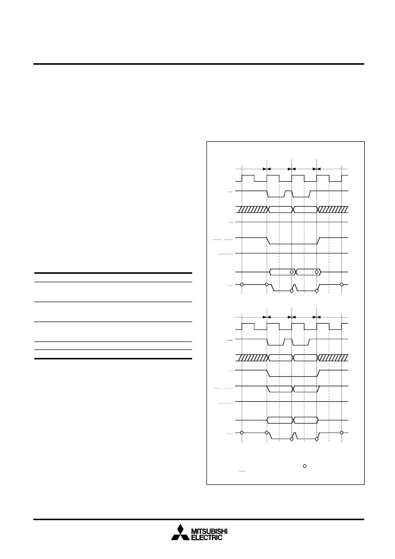
Read and write operations of the M32000D3FP are carried out using
the address bus, data bus, and the R/W, BCH, BCL and DC signals.
_______
BCL signals go to an "L" level. The CPU reads the data in the valid
byte positions. When writing, an "L" level is output from R/W, and
BCH and BCL are output according to the valid byte positions, so as
to specify the byte positions for writing into an external device.
Keep DC signal at the "H" level during idle cycles.
idle
read
"H"
"H"
CLKIN
BS
A8 - A30
SID, ST
BCH, BCL
BURST
D0 - D15
DC
R/W
idle
read
idle
write
idle
write
CLKIN
BS
A8 - A30
SID, ST
BCH, BCL
BURST
D0 - D15
DC
R/W
"H"
"Hi-z"
"Hi-z"
"Hi-z"
"Hi-z"
Note:
"Hi-z" means high-impedance, and indicates sampling timing.
Fig. 16 Read/write timing (two no-wait accesses)
Internal DRAM access control (CS)
The internal DRAM can be accessed when CS is driven to an "L"
level after the M32000D3FP enters the hold state (HACK = "L").
To access the internal DRAM from external, the following signals
from the system bus side should be controlled.
A8 to A30
Input internal DRAM addresses to be read or written.
BCH, BCL
Specify the byte position of data to be written into the internal
DRAM. BCH corresponds to the MSB side (D0 to D7), and BCL
corresponds to the LSB side (D8 to D15).
R/W
Specify read or write operation. When reading, R/W = "H". When
writing, R/W = "L".
D0 to D15
16-bit data I/O bus.
SID
When accessing the internal DRAM from an external bus mas-
ter, an "L" level is input to SID to specify user space.
DC
This signal notifies to an external bus master that the internal
DRAM access is complete. When access is complete, an "L"
level is output to DC.
Table 1 Pin condition in hold state
pin name
BCH, BCL
ST, R/W, BS, BURST
D0 - D15
pin condition or operation
high-impedance
output when internal DRAM is read
by an external bus master (CS = "L",
R/W = "H"), otherwise high-impedance
output when internal DRAM is
accessed by an external bus master
__
(CS = "L"), otherwise high-impedance
output "L"
normal operation
DC
HACK
other pins
相關PDF資料 |
PDF描述 |
|---|---|
| M32000D4 | SINGLE CHIP 32 BIT CMOS MICROCOMPUTER |
| M32000D4AFP | SINGLE CHIP 32 BIT CMOS MICROCOMPUTER |
| M32170F3VFP | SINGLE-CHIP 32-BIT CMOS MICROCOMPUTER |
| M32174F3VFP | SINGLE-CHIP 32-BIT CMOS MICROCOMPUTER |
| M32170F3VFG | 32-BIT RISC SINGLE-CHIP MICROCOMPUTER |
相關代理商/技術參數 |
參數描述 |
|---|---|
| M32000D4 | 制造商:MITSUBISHI 制造商全稱:Mitsubishi Electric Semiconductor 功能描述:SINGLE CHIP 32 BIT CMOS MICROCOMPUTER |
| M32000D4AFP | 制造商:MITSUBISHI 制造商全稱:Mitsubishi Electric Semiconductor 功能描述:SINGLE CHIP 32 BIT CMOS MICROCOMPUTER |
| M32000D4BFP-80 | 制造商:MITSUBISHI 制造商全稱:Mitsubishi Electric Semiconductor 功能描述:SINGLE-CHIP 32-BIT CMOS MICROCOMPUTER |
| M32002AGLJ | 制造商:MTRONPTI 制造商全稱:MTRONPTI 功能描述:9x14 mm, 3.3/2.5/1.8 Volt, PECL/LVDS/CML, VCXO |
| M32002AGMJ | 制造商:MTRONPTI 制造商全稱:MTRONPTI 功能描述:9x14 mm, 3.3/2.5/1.8 Volt, PECL/LVDS/CML, VCXO |
發(fā)布緊急采購,3分鐘左右您將得到回復。