- 您現(xiàn)在的位置:買(mǎi)賣(mài)IC網(wǎng) > PDF目錄44574 > LMX2335UTM/NOPB (NATIONAL SEMICONDUCTOR CORP) PLL FREQUENCY SYNTHESIZER, 1200 MHz, PDSO16 PDF資料下載
參數(shù)資料
| 型號(hào): | LMX2335UTM/NOPB |
| 廠商: | NATIONAL SEMICONDUCTOR CORP |
| 元件分類(lèi): | PLL合成/DDS/VCOs |
| 英文描述: | PLL FREQUENCY SYNTHESIZER, 1200 MHz, PDSO16 |
| 封裝: | PLASTIC, TSSOP-16 |
| 文件頁(yè)數(shù): | 47/48頁(yè) |
| 文件大?。?/td> | 3127K |
| 代理商: | LMX2335UTM/NOPB |
第1頁(yè)第2頁(yè)第3頁(yè)第4頁(yè)第5頁(yè)第6頁(yè)第7頁(yè)第8頁(yè)第9頁(yè)第10頁(yè)第11頁(yè)第12頁(yè)第13頁(yè)第14頁(yè)第15頁(yè)第16頁(yè)第17頁(yè)第18頁(yè)第19頁(yè)第20頁(yè)第21頁(yè)第22頁(yè)第23頁(yè)第24頁(yè)第25頁(yè)第26頁(yè)第27頁(yè)第28頁(yè)第29頁(yè)第30頁(yè)第31頁(yè)第32頁(yè)第33頁(yè)第34頁(yè)第35頁(yè)第36頁(yè)第37頁(yè)第38頁(yè)第39頁(yè)第40頁(yè)第41頁(yè)第42頁(yè)第43頁(yè)第44頁(yè)第45頁(yè)第46頁(yè)當(dāng)前第47頁(yè)第48頁(yè)
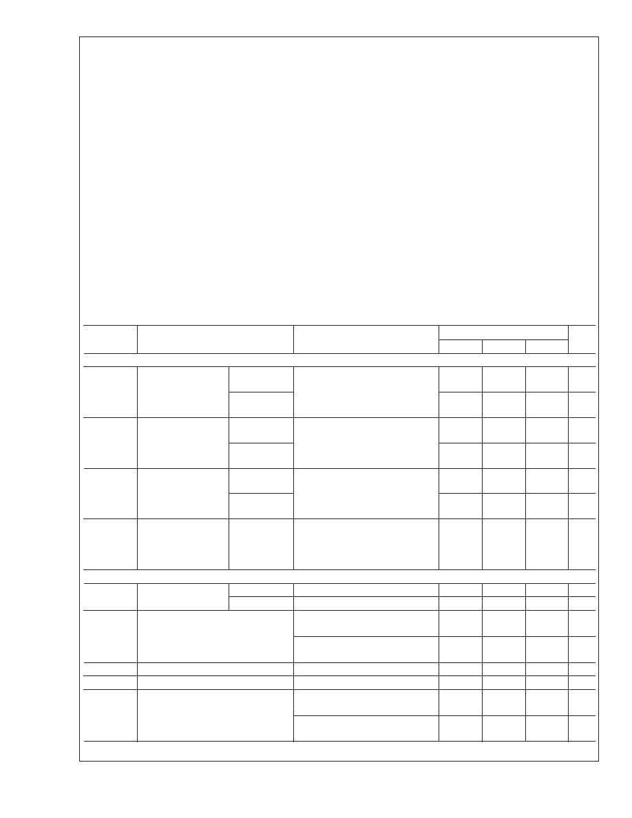
Absolute Maximum Ratings (Notes 1,
If Military/Aerospace specified devices are required,
please contact the National Semiconductor Sales Office/
Distributors for availability and specifications.
Power Supply Voltage
V
CC to GND
0.3V to +6.5V
V
P RF1 to GND
0.3V to +6.5V
V
P RF2 to GND
0.3V to +6.5V
Voltage on any pin to GND (V
I)
V
I must be < +6.5V
0.3V to V
CC+0.3V
Storage Temperature Range (T
S)
65C to +150C
Lead Temperature (solder 4 s) (T
L)
+260C
16-Pin TSSOP
θ
JA Thermal
Impedance
137.1C/W
20-Pin TSSOP
θ
JA Thermal
Impedance
114.5C/W
16-Pin CSP
θ
JA Thermal Impedance
130C/W
24-Pin CSP
θ
JA Thermal Impedance
112C/W
Recommended Operating
Conditions (Note 1)
Power Supply Voltage
V
CC to GND
+2.7V to +5.5V
V
P RF1 to GND
V
CC to +5.5V
V
P RF2 to GND
V
CC to +5.5V
Operating Temperature (T
A)
40C to +85C
Note 1: Absolute Maximum Ratings indicate limits beyond which damage to
the device may occur. Recommended Operating Conditions indicate condi-
tions for which the device is intended to be functional, but do not guarantee
specific performance limits. For guaranteed specifications and test condi-
tions, see the Electrical Characteristics. The guaranteed specifications apply
only for the test conditions listed.
Note 2: This device is a high performance RF integrated circuit with an ESD
rating <2 kV and is ESD sensitive. Handling and assembly of this device
should only be done at ESD protected work stations.
Note 3: GND=0V
Electrical Characteristics
V
CC =VP RF1=VP RF2 = 3.0V, 40C
≤ T
A
≤ +85C, unless otherwise specified
Symbol
Parameter
Conditions
Value
Units
Min
Typ
Max
I
CC PARAMETERS
I
CCRF1 + RF2
Power Supply
Current, RF1 + RF2
Synthesizers
LMX2335U
Clock, Data and LE = GND
OSC
in = GND
PWDN RF1 Bit = 0
PWDN RF2 Bit = 0
3.0
4.0
mA
LMX2336U
3.5
4.5
mA
I
CCRF1
Power Supply
Current, RF1
Synthesizer Only
LMX2335U
Clock, Data and LE = GND
OSC
in = GND
PWDN RF1 Bit = 0
PWDN RF2 Bit = 1
1.5
2.0
mA
LMX2336U
2.0
2.5
mA
I
CCRF2
Power Supply
Current, RF2
Synthesizer Only
LMX2335U
Clock, Data and LE = GND
OSC
in = GND
PWDN RF1 Bit = 1
PWDN RF2 Bit = 0
1.5
2.0
mA
LMX2336U
1.5
2.0
I
CC-PWDN
Powerdown Current
LMX2335U/
Clock, Data and LE = GND
OSC
in = GND
PWDN RF1 Bit = 1
PWDN RF2 Bit = 1
1.0
10.0
A
LMX2336U
RF1 SYNTHESIZER PARAMETERS
f
IN RF1
RF1 Operating
Frequency
LMX2335U
100
1200
MHz
LMX2336U
200
2000
MHz
N
RF1
RF1 N Divider Range
Prescaler = 64/65
192
131135
Prescaler = 128/129
384
262143
R
RF1
RF1 R Divider Range
3
32767
FφRF1
RF1 Phase Detector Frequency
10
MHz
Pf
IN RF1
RF1 Input Sensitivity
2.7V
≤ V
CC
≤ 3.0V
15
0
dBm
3.0V < V
CC
≤ 5.5V
10
0
dBm
LMX2335U/LMX2336U
www.national.com
8
相關(guān)PDF資料 |
PDF描述 |
|---|---|
| LMX2336MDA | PLL FREQUENCY SYNTHESIZER, 2000 MHz, UUC |
| LMX2346TM/NOPB | PLL FREQUENCY SYNTHESIZER, 2000 MHz, PDSO16 |
| LMX2346TMX/NOPB | PLL FREQUENCY SYNTHESIZER, 2000 MHz, PDSO16 |
| LMX2346SLBX/NOPB | PLL FREQUENCY SYNTHESIZER, 2000 MHz, CQCC16 |
| LMX2350TM/NOPB | PLL FREQUENCY SYNTHESIZER, 2500 MHz, PDSO24 |
相關(guān)代理商/技術(shù)參數(shù) |
參數(shù)描述 |
|---|---|
| LMX2335UTMX | 制造商:NSC 制造商全稱(chēng):National Semiconductor 功能描述:PLLatinum Ultra Low Power Dual Frequency Synthesizer for RF Personal Communications |
| LMX2336 | 制造商:NSC 制造商全稱(chēng):National Semiconductor 功能描述:PLLatinum⑩ Dual Frequency Synthesizer for RF Personal Communications |
| LMX2336 WAF | 制造商:Texas Instruments 功能描述: |
| LMX2336L | 制造商:NSC 制造商全稱(chēng):National Semiconductor 功能描述:PLLatinum⑩ Low Power Dual Frequency Synthesizer for RF Personal Communications |
| LMX2336LSLB | 制造商:NSC 制造商全稱(chēng):National Semiconductor 功能描述:PLLatinum⑩ Low Power Dual Frequency Synthesizer for RF Personal Communications |
發(fā)布緊急采購(gòu),3分鐘左右您將得到回復(fù)。