- 您現(xiàn)在的位置:買賣IC網(wǎng) > PDF目錄44574 > LMX2335UTM/NOPB (NATIONAL SEMICONDUCTOR CORP) PLL FREQUENCY SYNTHESIZER, 1200 MHz, PDSO16 PDF資料下載
參數(shù)資料
| 型號: | LMX2335UTM/NOPB |
| 廠商: | NATIONAL SEMICONDUCTOR CORP |
| 元件分類: | PLL合成/DDS/VCOs |
| 英文描述: | PLL FREQUENCY SYNTHESIZER, 1200 MHz, PDSO16 |
| 封裝: | PLASTIC, TSSOP-16 |
| 文件頁數(shù): | 25/48頁 |
| 文件大?。?/td> | 3127K |
| 代理商: | LMX2335UTM/NOPB |
第1頁第2頁第3頁第4頁第5頁第6頁第7頁第8頁第9頁第10頁第11頁第12頁第13頁第14頁第15頁第16頁第17頁第18頁第19頁第20頁第21頁第22頁第23頁第24頁當前第25頁第26頁第27頁第28頁第29頁第30頁第31頁第32頁第33頁第34頁第35頁第36頁第37頁第38頁第39頁第40頁第41頁第42頁第43頁第44頁第45頁第46頁第47頁第48頁
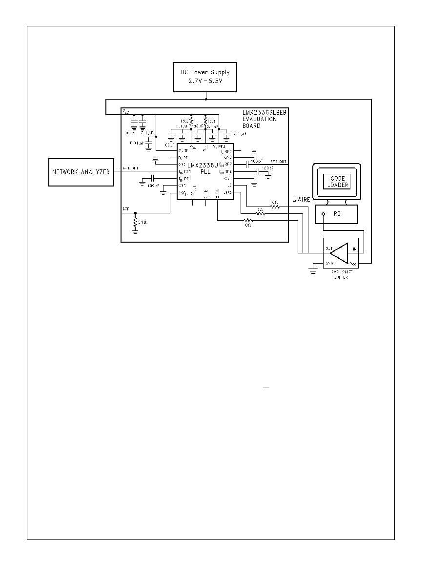
Test Setups (Continued)
LMX2335U and LMX2336U f
IN Impedance Test Setup
10136779
The block diagram above illustrates the setup required to
measure the LMX2336U device’s RF1 input impedance. The
RF2 input impedance and reference oscillator impedance
setups are very much similar. The same setup is used for a
LMX2336TMEB Evaluation Board. Measuring the device’s
input impedance facilitates the design of appropriate match-
ing networks to match the PLL to the VCO, or in more critical
situations, to the characteristic impedance of the printed
circuit board (PCB) trace, to prevent undesired transmission
line effects.
Before the actual measurements are taken, the Network
Analyzer needs to be calibrated, i.e. the error coefficients
need to be calculated. Therefore, three standards will be
used to calculate these coefficients: an open, short and a
matched load. A 1-port calibration is implemented here.
To calculate the coefficients, the PLL chip is first removed
from the PCB. The Network Analyzer port is then connected
to the RF1 OUT connector of the evaluation board and the
desired operating frequency is set. The typical frequency
range selected for the LMX2336U device’s RF1 synthesizer
is from 100 MHz to 2000 MHz. The standards will be located
down the length of the RF1 OUT transmission line. The
transmission line adds electrical length and acts as an offset
from the reference plane of the Network Analyzer; therefore,
it must be included in the calibration. Although not shown, 0
resistors are used to complete the RF1 OUT transmission
line (trace).
To implement an open standard, the end of the RF1 OUT
trace is simply left open. To implement a short standard, a 0
resistor is placed at the end of the RF1 OUT transmission
line. Last of all, to implement a matched load standard, two
100
resistors in parallel are placed at the end of the RF1
OUT transmission line. The Network Analyzer calculates the
calibration coefficients based on the measured S
11 param-
eters. With this all done, calibration is now complete.
The PLL chip is then placed on the PCB. A power supply is
connected to V
CC and the bias voltage is swept from 2.7V to
5.5V. The OSC
in pin is tied to the ground plane. Alternatively,
the OSC
in pin can be tied to VCC. In this setup, the comple-
mentary input (f
IN RF1) is AC coupled to ground. With the
Network Analyzer still connected to RF1 OUT, the measured
f
IN RF1 impedance is displayed.
Note: The impedance of the reference oscillator is measured
when the oscillator buffer is powered up (PWDN RF1 Bit = 0
or PWDN RF2 Bit = 0), and when the oscillator buffer is
powered down (PWDN RF1 Bit = 1 and PWDN RF2 Bit = 1).
The LMX2335U f
IN impedance test setup is very much simi-
lar to the above test setup. Note that there are no comple-
mentary inputs in the LMX2335U device.
LMX2335U/LMX2336U
www.national.com
31
相關(guān)PDF資料 |
PDF描述 |
|---|---|
| LMX2336MDA | PLL FREQUENCY SYNTHESIZER, 2000 MHz, UUC |
| LMX2346TM/NOPB | PLL FREQUENCY SYNTHESIZER, 2000 MHz, PDSO16 |
| LMX2346TMX/NOPB | PLL FREQUENCY SYNTHESIZER, 2000 MHz, PDSO16 |
| LMX2346SLBX/NOPB | PLL FREQUENCY SYNTHESIZER, 2000 MHz, CQCC16 |
| LMX2350TM/NOPB | PLL FREQUENCY SYNTHESIZER, 2500 MHz, PDSO24 |
相關(guān)代理商/技術(shù)參數(shù) |
參數(shù)描述 |
|---|---|
| LMX2335UTMX | 制造商:NSC 制造商全稱:National Semiconductor 功能描述:PLLatinum Ultra Low Power Dual Frequency Synthesizer for RF Personal Communications |
| LMX2336 | 制造商:NSC 制造商全稱:National Semiconductor 功能描述:PLLatinum⑩ Dual Frequency Synthesizer for RF Personal Communications |
| LMX2336 WAF | 制造商:Texas Instruments 功能描述: |
| LMX2336L | 制造商:NSC 制造商全稱:National Semiconductor 功能描述:PLLatinum⑩ Low Power Dual Frequency Synthesizer for RF Personal Communications |
| LMX2336LSLB | 制造商:NSC 制造商全稱:National Semiconductor 功能描述:PLLatinum⑩ Low Power Dual Frequency Synthesizer for RF Personal Communications |
發(fā)布緊急采購,3分鐘左右您將得到回復。