- 您現(xiàn)在的位置:買賣IC網(wǎng) > PDF目錄358878 > LM9830 (National Semiconductor Corporation) LM9830 36-Bit Color Document Scanner PDF資料下載
參數(shù)資料
| 型號: | LM9830 |
| 廠商: | National Semiconductor Corporation |
| 英文描述: | LM9830 36-Bit Color Document Scanner |
| 中文描述: | LM9830 36位彩色文件掃描儀 |
| 文件頁數(shù): | 23/45頁 |
| 文件大小: | 566K |
| 代理商: | LM9830 |
第1頁第2頁第3頁第4頁第5頁第6頁第7頁第8頁第9頁第10頁第11頁第12頁第13頁第14頁第15頁第16頁第17頁第18頁第19頁第20頁第21頁第22頁當前第23頁第24頁第25頁第26頁第27頁第28頁第29頁第30頁第31頁第32頁第33頁第34頁第35頁第36頁第37頁第38頁第39頁第40頁第41頁第42頁第43頁第44頁第45頁
23
http://www.national.com
Applications Information
1.0 THEORY OF OPERATION
1.1 Overview
A scanner is composed of many different but tightly intercon-
nected blocks (the analog front end and ADC, sensor clock gen-
eration, stepper motor control, data buffering, parallel port I/O,
and others).
1.2 Signal Processing Overview
1.3 Scanner Support Functions Overview
2.0 Signal Processing Operation
2.1 ADC
The ADC is a 6MHz 12 bit pipelined architecture.
2.2 Pixel Rate Offset Correction Block
Two bytes are used to store the pixel rate offset and gain coeffi-
cients for each pixel. For CCDs, the split is usually 6 bits for offset
and 10 bits for gain. For some CIS sensors with unusually large
offsets, the offset correction range may be increased by changing
the split to 8 bits for offset and 8 bits for gain. This split is deter-
mined by a bit in the configuration register.
A digital subtractor subtracts the 6 (or 8) bit offset word (corre-
sponding to that pixel’s offset error) from each pixel. The LSB of
the offset word is the same size as the 10 bit LSB of the ADC (the
two smallest 12 bit ADC output bits, D1 and D0, are not used with
the offset subtractor). The coefficients are stored in the external
RAM and accessed at the pixel rate.
The subtractor saturates at 0, i.e. if the coefficient to be sub-
tracted is greater than the ADC output code, the result is an out-
put of 0.
2.3 Pixel Rate Gain Correction Block
This is a digital multiplier that multiplies the output word from the
subtractor by a 10 (or 8) bit digital correction coefficient corre-
sponding to that pixel’s gain error. The coefficients are stored in
the external RAM and accessed at the pixel rate. When in 8 bit
mode, the 8 bits correspond to the top 8 MSBs of the 10 bit digital
correction coefficient word. The 10 bit LSBs of the input word are
padded with 0s in 8 bit mode.
The multiplier saturates at 1023, i.e. if the result of the multiplica-
tion is greater than 1023, the multiplier output is 1023.
2.4 Pixel Processing Block
2.4.1 Pixel Processing In 8/24 Bit Mode
In the 8 and 10 bit output modes (for 24 and 30 bit color scans),
this stage is where the optical resolution of the sensor is digitally
reduced.
To maximize scanning speed and image quality at the popular
resolutions of 400, 300, 200, 150, 100, 75, and 50 dpi, the resolu-
tion can be reduced inside the scanner, prior to the gamma cor-
rection stage. (Resolution in the vertical direction is controlled by
the stepper motor speed.) This is done by averaging adjacent pix-
els. For example, to get 100 dpi from a 300dpi optical sensor, you
would average 3 300dpi pixels:
The number of pixels out of the Pixel Processing block is equal to
the integer portion of the number of pixels in to the Pixel Process-
ing block divided by the “Divide By” setting, from the table shown
in Figure 11.
If there are not enough pixels at the end of a line to form a com-
plete pixel, the last pixel will be eliminated. For example, if a line
is 35 pixels wide and the Horizontal DPI setting is set to divide by
6, then the output of the Pixel Processing block will be 5 pixels
(the integer portion of 35/6). The last 5 pixels will be discarded,
since 6 pixels would be required to form a new pixel in this mode.
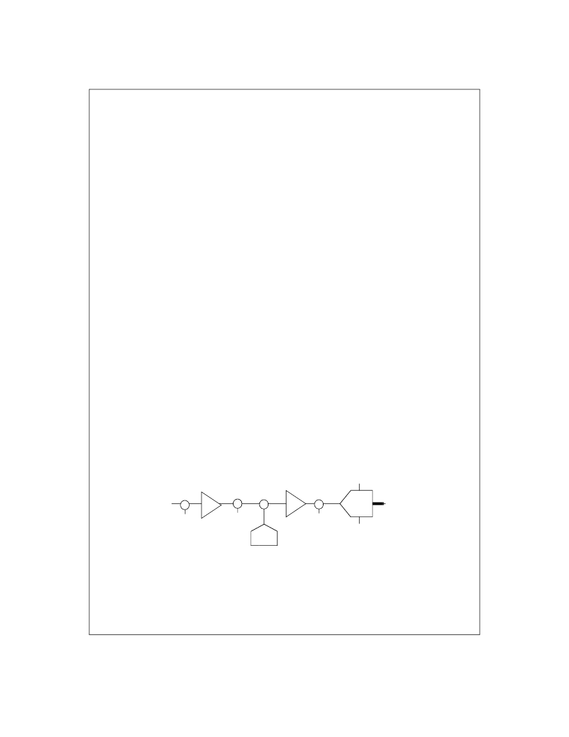
Figure 10: Analog Front End (AFE) Model
V
DAC
DAC
Offset
G
PGA
Σ
+
+
12 Bit
ADC
+
+
+
+
V
OS3
V
OS2
Σ
Σ
D
OUT
G
B
+
+
V
OS1
V
IN
Σ
Boost
1V/V or
3V/V
PGA
0.93V/V to
3V/V
D
OUT
= (((V
IN
+ V
OS1
)G
B
+ V
DAC
+ V
OS2
)G
PGA
+ V
OS1
)C
simplified, with all offsets = 0, this is:
D
OUT
= (V
IN
G
B
+ V
DAC
)G
PGA
C
C is a constant that combines the gain error through the AFE, reference voltage variance, and analog voltage
to digital code conversion into one constant. Ideally, C = 2048 codes/V (4096codes/2V). Manufacturing toler-
ances widen the range of C. See Electrical Specifications
pixel100dpi
pn-2
pn-1
3
pn
+
+
=
PixelsOUT
INT
Divide By
=
相關(guān)PDF資料 |
PDF描述 |
|---|---|
| LM98503CCVV | 10-Bit, 18 MSPS Camera Signal Processor |
| LM98503 | 10-Bit, 18 MSPS Camera Signal Processor |
| LM99CIMM | 【1C Accurate, High Temperature, Remote Diode Temperature Sensor with Two-Wire Interface |
| LM99CIMMX | 【1C Accurate, High Temperature, Remote Diode Temperature Sensor with Two-Wire Interface |
| LM9V381 | Color STN-LCD Module |
相關(guān)代理商/技術(shù)參數(shù) |
參數(shù)描述 |
|---|---|
| LM9830VJD | 功能描述:視頻模擬/數(shù)字化轉(zhuǎn)換器集成電路 RoHS:否 制造商:Texas Instruments 輸入信號類型:Differential 轉(zhuǎn)換器數(shù)量:1 ADC 輸入端數(shù)量:4 轉(zhuǎn)換速率:3 Gbps 分辨率:8 bit 結(jié)構(gòu): 輸入電壓:3.3 V 接口類型:SPI 信噪比: 電壓參考: 電源電壓-最大:3.45 V 電源電壓-最小:3.15 V 最大功率耗散: 最大工作溫度:+ 85 C 最小工作溫度:- 40 C 封裝 / 箱體:TCSP-48 封裝:Reel |
| LM9830VJD/NOPB | 功能描述:視頻模擬/數(shù)字化轉(zhuǎn)換器集成電路 RoHS:否 制造商:Texas Instruments 輸入信號類型:Differential 轉(zhuǎn)換器數(shù)量:1 ADC 輸入端數(shù)量:4 轉(zhuǎn)換速率:3 Gbps 分辨率:8 bit 結(jié)構(gòu): 輸入電壓:3.3 V 接口類型:SPI 信噪比: 電壓參考: 電源電壓-最大:3.45 V 電源電壓-最小:3.15 V 最大功率耗散: 最大工作溫度:+ 85 C 最小工作溫度:- 40 C 封裝 / 箱體:TCSP-48 封裝:Reel |
| LM9830VJDX | 制造商:NSC 制造商全稱:National Semiconductor 功能描述:LM9830 36-Bit Color Document Scanner |
| LM9831 | 制造商:NSC 制造商全稱:National Semiconductor 功能描述:LM9831 42-Bit Color, 1200dpi USB Image Scanner |
| LM9831CCVJD | 制造商:NSC 制造商全稱:National Semiconductor 功能描述:LM9831 42-Bit Color, 1200dpi USB Image Scanner |
發(fā)布緊急采購,3分鐘左右您將得到回復。