- 您現(xiàn)在的位置:買賣IC網(wǎng) > PDF目錄299403 > LFXP20E-5FN484C (LATTICE SEMICONDUCTOR CORP) PDF資料下載
參數(shù)資料
| 型號: | LFXP20E-5FN484C |
| 廠商: | LATTICE SEMICONDUCTOR CORP |
| 元件分類: | FPGA |
| 中文描述: | FPGA, 2464 CLBS, PBGA484 |
| 封裝: | 23 X 23 MM, LEAD FREE, FPBGA-484 |
| 文件頁數(shù): | 24/130頁 |
| 文件大小: | 1312K |
| 代理商: | LFXP20E-5FN484C |
第1頁第2頁第3頁第4頁第5頁第6頁第7頁第8頁第9頁第10頁第11頁第12頁第13頁第14頁第15頁第16頁第17頁第18頁第19頁第20頁第21頁第22頁第23頁當前第24頁第25頁第26頁第27頁第28頁第29頁第30頁第31頁第32頁第33頁第34頁第35頁第36頁第37頁第38頁第39頁第40頁第41頁第42頁第43頁第44頁第45頁第46頁第47頁第48頁第49頁第50頁第51頁第52頁第53頁第54頁第55頁第56頁第57頁第58頁第59頁第60頁第61頁第62頁第63頁第64頁第65頁第66頁第67頁第68頁第69頁第70頁第71頁第72頁第73頁第74頁第75頁第76頁第77頁第78頁第79頁第80頁第81頁第82頁第83頁第84頁第85頁第86頁第87頁第88頁第89頁第90頁第91頁第92頁第93頁第94頁第95頁第96頁第97頁第98頁第99頁第100頁第101頁第102頁第103頁第104頁第105頁第106頁第107頁第108頁第109頁第110頁第111頁第112頁第113頁第114頁第115頁第116頁第117頁第118頁第119頁第120頁第121頁第122頁第123頁第124頁第125頁第126頁第127頁第128頁第129頁第130頁
2-9
Architecture
Lattice Semiconductor
LatticeXP Family Data Sheet
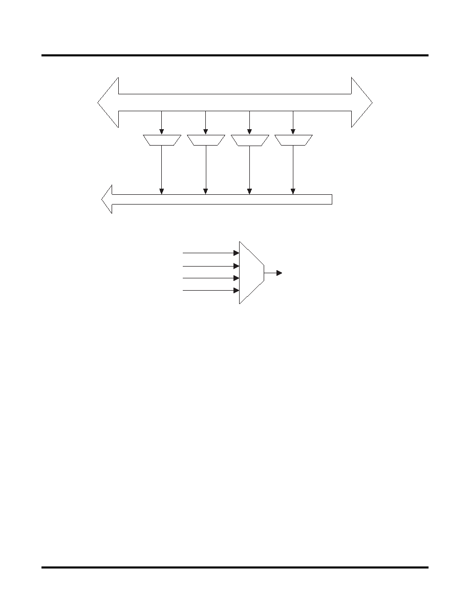
Figure 2-8. Per Quadrant Secondary Clock Selection
Figure 2-9. Slice Clock Selection
sysCLOCK Phase Locked Loops (PLLs)
The PLL clock input, from pin or routing, feeds into an input clock divider. There are three sources of feedback sig-
nals to the feedback divider: from CLKOP (PLL internal), from clock net (CLKOP or CLKOS) or from a user clock
(PIN or logic). There is a PLL_LOCK signal to indicate that VCO has locked on to the input clock signal. Figure 2-
10 shows the sysCLOCK PLL diagram.
The setup and hold times of the device can be improved by programming a delay in the feedback or input path of
the PLL which will advance or delay the output clock with reference to the input clock. This delay can be either pro-
grammed during configuration or can be adjusted dynamically. In dynamic mode, the PLL may lose lock after
adjustment and not relock until the tLOCK parameter has been satisfied. Additionally, the phase and duty cycle block
allows the user to adjust the phase and duty cycle of the CLKOS output.
The sysCLOCK PLLs provide the ability to synthesize clock frequencies. Each PLL has four dividers associated
with it: input clock divider, feedback divider, post scalar divider and secondary clock divider. The input clock divider
is used to divide the input clock signal, while the feedback divider is used to multiply the input clock signal. The post
scalar divider allows the VCO to operate at higher frequencies than the clock output, thereby increasing the fre-
quency range. The secondary divider is used to derive lower frequency outputs.
4 Secondary Clocks per Quadrant
20 Secondary Clock Feedlines : 4 Clock Input Pads + 16 Routing Signals
Primary Clock
Secondary Clock
Routing
Clock to Each Slice
GND
相關PDF資料 |
PDF描述 |
|---|---|
| LFXP15C-4FN256C | |
| LFZ3508VXX | GENERAL PURPOSE INDUCTOR |
| LFZ2805HXX | GENERAL PURPOSE INDUCTOR |
| LF02004VTX | GENERAL PURPOSE INDUCTOR |
| LG3341-NE7501 | T-1 SINGLE COLOR LED, GREEN, 3 mm |
相關代理商/技術參數(shù) |
參數(shù)描述 |
|---|---|
| LFXP217E5CF484C | 制造商:LATTICE 制造商全稱:Lattice Semiconductor 功能描述:LatticeXP2 Family Data Sheet |
| LFXP217E5CF484I | 制造商:LATTICE 制造商全稱:Lattice Semiconductor 功能描述:LatticeXP2 Family Data Sheet |
| LFXP217E5CF672C | 制造商:LATTICE 制造商全稱:Lattice Semiconductor 功能描述:LatticeXP2 Family Data Sheet |
| LFXP217E5CF672I | 制造商:LATTICE 制造商全稱:Lattice Semiconductor 功能描述:LatticeXP2 Family Data Sheet |
| LFXP217E5CFN484C | 制造商:LATTICE 制造商全稱:Lattice Semiconductor 功能描述:LatticeXP2 Family Data Sheet |
發(fā)布緊急采購,3分鐘左右您將得到回復。