- 您現(xiàn)在的位置:買賣IC網(wǎng) > PDF目錄358757 > LC66358B (Sanyo Electric Co.,Ltd.) Four-bit Single-Chip Microcontrollers On-Chip 8 K-byte ROM(4位單片微控制器(帶8K字節(jié)片上ROM)) PDF資料下載
參數(shù)資料
| 型號: | LC66358B |
| 廠商: | Sanyo Electric Co.,Ltd. |
| 英文描述: | Four-bit Single-Chip Microcontrollers On-Chip 8 K-byte ROM(4位單片微控制器(帶8K字節(jié)片上ROM)) |
| 中文描述: | 四位單芯片微控制器片8的K -字節(jié)的光盤(4位單片微控制器(帶8K的字節(jié)片上光盤)) |
| 文件頁數(shù): | 9/23頁 |
| 文件大小: | 267K |
| 代理商: | LC66358B |
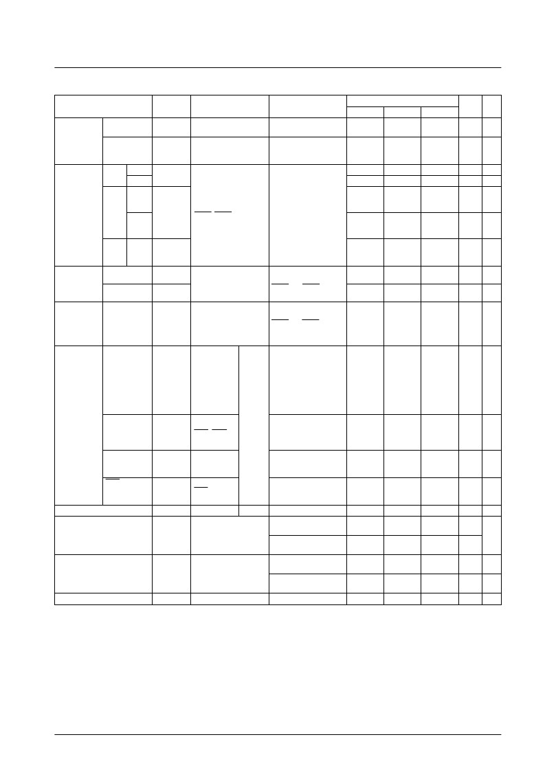
Continued from preceding page.
Note: 1. Common input and output ports with open-drain output specifications are specified for the state with the output n-channel transistor turned off.
These pins cannot be used for input when the CMOS output specification option is selected.
2. Common input and output ports with open-drain output specifications are specified for the state with the output n-channel transistor turned off.
Ratings for pull-up output specification pins are stipulated for the output pull-up current I
PO
. These pins cannot be used for input when the CMOS
output specification option is selected.
3. Stipulated for CMOS output specifications with the output n-channel transistor in the off state.
4. Stipulated for pull-up output specifications with the output n-channel transistor in the off state.
5. Stipulated for open-drain output specifications with the output n-channel transistor in the off state.
6. In the reset state
No. 4677-9/23
LC66354B, 66356B, 66358B
Parameter
Symbol
Applicable pins
Conditions
Ratings
Unit
Note
min
typ
max
Oscillator
frequency
f
CF
OSC1, OSC2
Figure 2, 4 MHz
4.0
MHz
Ceramic
oscillator
Oscillator
stabilization
time
f
CFS
Figure 3, 4 MHz
10
ms
Cycle
time
Input
t
CKCY
0.9
μs
Output
2.0
Tcyc
Low
level/
high
level
pulse
widths
Input
t
CKL
0.4
μs
Serial clock
SCK0, SCK1
Output
t
CKH
1.0
Tcyc
Rise/
fall
times
t
CKR
t
CKF
Output
0.1
μs
Data setup time
t
ICK
Stipulated with respect to
the rising edge timing for
SCK0 and SCK1 from
Figure 4
0.3
μs
Serial input
SI0, SI1
Data hold time
t
CKI
0.3
μs
Stipulated with respect to
the rising edge timing for
SCK0 and SCK1 from
Figure 4 and the test load
shown in Figure 5
Output delay
time
Serial output
t
CKO
SO0, SO1
0.3
μs
INT0 high/low
level pulse
widths
t
IOH
t
IOL
INT0
2
Tcyc
Pulse
conditions
High/low level
pulse widths for
interrupt inputs
other than INT0
Figure 6
t
IIH
t
IIL
INT1, INT2
2
Tcyc
PIN1 high/low
level pulse
widths
t
PINH
t
PINL
PIN1
2
Tcyc
RES high/low
level pulse
widths
t
RSH
t
RSL
RES
3
Tcyc
Comparator response speed
T
RS
PD
Figure 7
20
ms
Using a 4 MHz ceramic
oscillator
3.0
5.0
mA
Operating mode current drain
I
DD OP
V
DD
8
Using a 4 MHz external
clock
3.0
5.0
mA
Using a 4 MHz ceramic
oscillator
1.0
2.0
mA
HALT mode current drain
I
DDHALT
V
DD
Using a 4 MHz external
clock
1.0
2.0
mA
Hold-mode current drain
I
DDHOLD
V
DD
V
DD
= 1.8 to 5.5 V
0.01
10
μA
The timing from Figure 4
and the test load from
Figure 5
Conditions such that
the INT0 interrupt is
accepted
Conditions such that
timer 0 event counter
and pulse width
measurement inputs
are accepted.
Conditions such that
all interrupts are
accepted
Conditions such that
timer 1 event counter
inputs are accepted.
Conditions such that
reset occurs
相關PDF資料 |
PDF描述 |
|---|---|
| LC66358S | Four-Bit Single-Chip Microcontrollers with 6k and 8k of On-Chip ROM |
| LC66358V | 3-Line to 8-Line Decoder / Demultiplexer 16-TVSOP -40 to 85 |
| LC66404A | 3-Line to 8-Line Decoder / Demultiplexer 16-TVSOP -40 to 85 |
| LC66506 | 6K-Byte/8K-Byte ROM-Contained Single-Chip 4-bit Microcomputer for Control-Oriented Applications |
| LC66512 | Dual Low-Noise Rail-To-Rail Operational Amplifier 8-TSSOP |
相關代理商/技術參數(shù) |
參數(shù)描述 |
|---|---|
| LC66358C | 制造商:SANYO 制造商全稱:Sanyo Semicon Device 功能描述:Four-Bit Single-Chip Microcontrollers with 4, 6, and 8 KB of On-Chip ROM |
| LC66358S | 制造商:SANYO 制造商全稱:Sanyo Semicon Device 功能描述:Four-Bit Single-Chip Microcontroller with 16 KB of On-Chip OTP PROM |
| LC66358V | 制造商:SANYO 制造商全稱:Sanyo Semicon Device 功能描述:4-bit Microcontroller with Built-in PROM |
| LC66404A | 制造商:SANYO 制造商全稱:Sanyo Semicon Device 功能描述:Four-Bit Single-Chip Microcontrollers with 8, 12, and 16 KB of On-Chip ROM |
| LC66406A | 制造商:SANYO 制造商全稱:Sanyo Semicon Device 功能描述:Four-Bit Single-Chip Microcontroller with 16 KB of On-Chip OTP PROM |
發(fā)布緊急采購,3分鐘左右您將得到回復。