- 您現(xiàn)在的位置:買賣IC網(wǎng) > PDF目錄384585 > L6726ATR (意法半導體) Single phase PWM controller PDF資料下載
參數(shù)資料
| 型號: | L6726ATR |
| 廠商: | 意法半導體 |
| 英文描述: | Single phase PWM controller |
| 中文描述: | 單相PWM控制器 |
| 文件頁數(shù): | 19/24頁 |
| 文件大小: | 399K |
| 代理商: | L6726ATR |

L6726A
Application details
19/24
section far from the controller without losing performances. Anyway, when possible, it is
recommended to minimize the distance between controller and power section. See
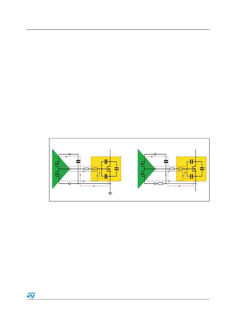
Figure 11
for drivers current paths.
Small signal components and connections to critical nodes of the application, as well as
bypass capacitors for the device supply, are also important. Locate bypass capacitor (VCC
and Bootstrap capacitor) and loop compensation components as close to the device as
practical. For over current programmability, place R
OCSET
close to the device and avoid
leakage current paths on LGATE / OC pin, since the internal current source is only 10
μ
A
Systems that do not use Schottky diode in parallel to the Low-Side MOSFET might show big
negative spikes on the PHASE pin. This spike must be limited within the absolute maximum
ratings (for example, adding a gate resistor in series to HS MOSFET gate, or a phase
resistor in series to PHASE pin), as well as the positive spike, but has an additional
consequence: it causes the bootstrap capacitor to be over-charged. This extra-charge can
cause, in the worst case condition of maximum input voltage and during particular
transients, that boot-to-phase voltage overcomes the absolute maximum ratings also
causing device failures. It is then suggested in this case to limit this extra-charge by adding a
small resistor in series to the bootstrap diode (R
D
in
Figure 1
).
Figure 11.
Drivers turn-on and turn-off paths
R
GATE
R
INT
C
GD
C
GS
C
DS
VCC
LS DRIVER
LS MOSFET
GND
LGATE
R
GATE
R
INT
C
GD
C
GS
C
DS
BOOT
HS DRIVER
HS MOSFET
PHASE
UGATE
R
PHASE
相關PDF資料 |
PDF描述 |
|---|---|
| L6727 | Single phase PWM controller |
| L6727TR | Single phase PWM controller |
| L6730CQ | Adjustable step-down controller with synchronous rectification |
| L6730C | Adjustable step-down controller with synchronous rectification |
| L6730CQTR | Adjustable step-down controller with synchronous rectification |
相關代理商/技術參數(shù) |
參數(shù)描述 |
|---|---|
| L6726-D18-T | 制造商:UTC-IC 制造商全稱:UTC-IC 功能描述:UNIVERSAL SPEECH CIRCUIT |
| L6726G-D18-T | 制造商:UTC-IC 制造商全稱:UTC-IC 功能描述:UNIVERSAL SPEECH CIRCUIT |
| L6726G-S18-R | 制造商:UTC-IC 制造商全稱:UTC-IC 功能描述:UNIVERSAL SPEECH CIRCUIT |
| L6726G-S18-T | 制造商:UTC-IC 制造商全稱:UTC-IC 功能描述:UNIVERSAL SPEECH CIRCUIT |
| L6726L-D18-T | 制造商:UTC-IC 制造商全稱:UTC-IC 功能描述:UNIVERSAL SPEECH CIRCUIT |
發(fā)布緊急采購,3分鐘左右您將得到回復。