- 您現(xiàn)在的位置:買賣IC網(wǎng) > PDF目錄373177 > KS16114 (SAMSUNG SEMICONDUCTOR CO. LTD.) 9600/14400 bps FAX MODEM PDF資料下載
參數(shù)資料
| 型號(hào): | KS16114 |
| 廠商: | SAMSUNG SEMICONDUCTOR CO. LTD. |
| 英文描述: | 9600/14400 bps FAX MODEM |
| 中文描述: | 14400分之9600基點(diǎn)傳真調(diào)制解調(diào)器 |
| 文件頁(yè)數(shù): | 4/69頁(yè) |
| 文件大小: | 513K |
| 代理商: | KS16114 |
第1頁(yè)第2頁(yè)第3頁(yè)當(dāng)前第4頁(yè)第5頁(yè)第6頁(yè)第7頁(yè)第8頁(yè)第9頁(yè)第10頁(yè)第11頁(yè)第12頁(yè)第13頁(yè)第14頁(yè)第15頁(yè)第16頁(yè)第17頁(yè)第18頁(yè)第19頁(yè)第20頁(yè)第21頁(yè)第22頁(yè)第23頁(yè)第24頁(yè)第25頁(yè)第26頁(yè)第27頁(yè)第28頁(yè)第29頁(yè)第30頁(yè)第31頁(yè)第32頁(yè)第33頁(yè)第34頁(yè)第35頁(yè)第36頁(yè)第37頁(yè)第38頁(yè)第39頁(yè)第40頁(yè)第41頁(yè)第42頁(yè)第43頁(yè)第44頁(yè)第45頁(yè)第46頁(yè)第47頁(yè)第48頁(yè)第49頁(yè)第50頁(yè)第51頁(yè)第52頁(yè)第53頁(yè)第54頁(yè)第55頁(yè)第56頁(yè)第57頁(yè)第58頁(yè)第59頁(yè)第60頁(yè)第61頁(yè)第62頁(yè)第63頁(yè)第64頁(yè)第65頁(yè)第66頁(yè)第67頁(yè)第68頁(yè)第69頁(yè)
KS16112/4
9600/14400 bps FAX MODEM
-
4
-
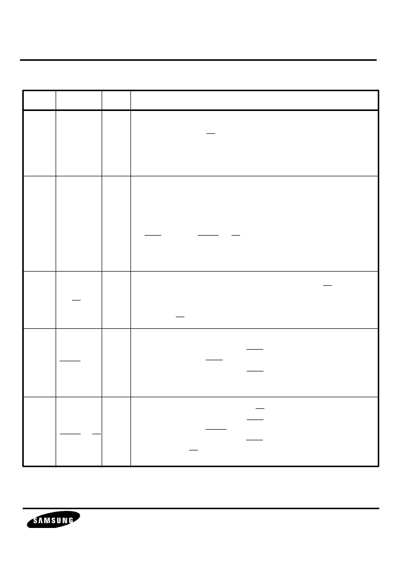
PIN DESCRIPTION
Pin No.
Symbol
Type
Description
67
1
2
3
4
55
56
57
58
59
60
61
62
65
66
64
RS4
RS3
RS2
RS1
RS0
D7
D6
D5
D4
D3
D2
D1
D0
CS
READ -
2
WRITE -R/W
I
I/O
I
I
I
Register select bus
These lines are used to address interface memory registers within
the modem. When CS is active, the modem decodes RS0 through
RS4 to address one of its 32 internal interface memory registers.
RS4 is the most significant bit. In a typical design, RS0 - RS4 are
connected to A0 - A4 address lines of the host microprocessor.
Data bus
These bi-directional data bus lines provide parallel data transfer
between the modem and the host microprocessor.
D7 is the most significant bit.
The direction of the D0 - D7 data bus is controlled by the
READ -
2
and WRITE - R/W signals.
When not being written into or read from, D0 - D7 assume the
high impedance state.
Chip select
The modem is selected and decodes RS0 - RS4 when CS
becomes active at which time data transfer between the modem
and the host can take place over the parallel data bus.
Typically, CS is driven by address decode logic.
Read enable ( bus mode ) or phase2 ( 6500 bus mode )
If 8085 bus mode is selected ( EN85 is connected to ground ), this
signal acts as the READ input.
If 6500 bus mode is selected ( EN85 is pulled - up to +5V ), this signal
acts as the Phase 2 clock input.
Write enable ( bus mode ) or R/W ( 6500 bus mode )
If 8085 bus mode is selected ( EN85 is connected to ground ), this
signal acts as the WRITE input.
If 6500 bus mode is selected ( EN85 is pulled - up to +5V ), this signal
acts as the R/W strobe.
相關(guān)PDF資料 |
PDF描述 |
|---|---|
| KS16112 | CAP 33PF 50V 5% NPO(C0G) SMD-0603 TR-7-PA |
| KS16116-02 | 9600 bps FAX MODEM(9600bps傳真調(diào)制解調(diào)器) |
| KS16117-02 | 14400 bps FAX MODEM(14400bps傳真調(diào)制解調(diào)器) |
| KS16118 | 9600bps FAX super one-chip(9600bps傳真調(diào)制解調(diào)器) |
| KS16120B | DSP for Digital Answering Phone(用于數(shù)字應(yīng)答電話的DSP) |
相關(guān)代理商/技術(shù)參數(shù) |
參數(shù)描述 |
|---|---|
| KS16-14 | 制造商:MAJOR 功能描述: |
| KS-16287L1 | 制造商:WSTELC 功能描述: |
| KS-16287L2 | 制造商:WSTELC 功能描述: |
| KS16390 | 制造商: 功能描述: 制造商:Cornell Dubilier Electronics 功能描述: 制造商:undefined 功能描述: |
| KS16479 | 制造商:Olympic Controls Corporation 功能描述: |
發(fā)布緊急采購(gòu),3分鐘左右您將得到回復(fù)。