- 您現(xiàn)在的位置:買賣IC網(wǎng) > PDF目錄374284 > K4T1G164QM-ZCD5 (SAMSUNG SEMICONDUCTOR CO. LTD.) 1Gb M-die DDR2 SDRAM Specification PDF資料下載
參數(shù)資料
| 型號(hào): | K4T1G164QM-ZCD5 |
| 廠商: | SAMSUNG SEMICONDUCTOR CO. LTD. |
| 英文描述: | 1Gb M-die DDR2 SDRAM Specification |
| 中文描述: | 1Gb的的M -模DDR2 SDRAM的規(guī)格 |
| 文件頁數(shù): | 19/28頁 |
| 文件大?。?/td> | 612K |
| 代理商: | K4T1G164QM-ZCD5 |
第1頁第2頁第3頁第4頁第5頁第6頁第7頁第8頁第9頁第10頁第11頁第12頁第13頁第14頁第15頁第16頁第17頁第18頁當(dāng)前第19頁第20頁第21頁第22頁第23頁第24頁第25頁第26頁第27頁第28頁
Page 19 of 28
Rev. 1.1 Aug. 2005
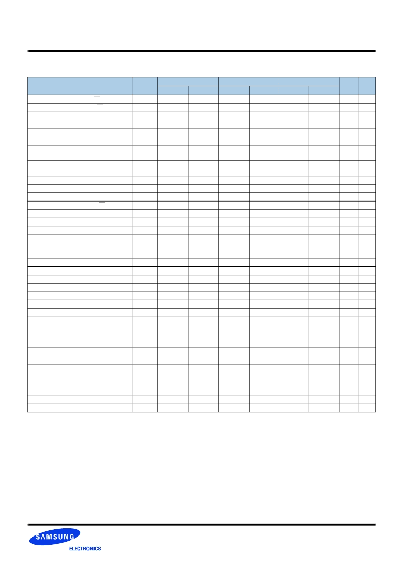
DDR2 SDRAM
1G A-die DDR2 SDRAM
Timing Parameters by Speed Grade
(Refer to notes for informations related to this table at the bottom)
Parameter
Symbol
DDR2-667
DDR2-533
DDR2-400
Units Notes
min
max
min
max
min
max
DQ output access time from CK/CK
tAC
-450
+450
-500
+500
-600
+600
ps
DQS output access time from CK/CK
tDQSCK
-400
+400
-450
+450
-500
+500
ps
CK high-level width
tCH
0.45
0.55
0.45
0.55
0.45
0.55
tCK
CK low-level width
tCL
0.45
0.55
0.45
0.55
0.45
0.55
tCK
CK half period
tHP
min(tCL, tCH)
x
min(tCL, tCH)
x
min(tCL, tCH)
x
ps
20,21
Clock cycle time, CL=x
tCK
3000
8000
3750
8000
5000
8000
ps
24
DQ and DM input hold time
tDH(base)
175
x
225
x
275
x
ps
15,16,
17,20
DQ and DM input setup time
tDS(base)
100
x
100
x
150
x
ps
15,16,
17,21
Control & Address input pulse width for each input
tIPW
0.6
x
0.6
x
0.6
x
tCK
DQ and DM input pulse width for each input
tDIPW
0.35
x
0.35
x
0.35
x
tCK
Data-out high-impedance time from CK/CK
tHZ
x
tAC max
x
tAC max
x
tAC max
ps
DQS low-impedance time from CK/CK
tLZ(DQS)
tAC min
tAC max
tAC min
tAC max
tAC min
tAC max
ps
27
DQ low-impedance time from CK/CK
tLZ(DQ)
2*tAC min
tAC max
2* tACmin
tAC max
2* tACmin
tAC max
ps
27
DQS-DQ skew for DQS and associated DQ signals tDQSQ
x
240
x
300
x
350
ps
22
DQ hold skew factor
tQHS
x
340
x
400
x
450
ps
21
DQ/DQS output hold time from DQS
tQH
tHP - tQHS
x
tHP - tQHS
x
tHP - tQHS
x
ps
First DQS latching transition to associated clock
edge
tDQSS
-0.25
0.25
-0.25
0.25
-0.25
0.25
tCK
DQS input high pulse width
tDQSH
0.35
x
0.35
x
0.35
x
tCK
DQS input low pulse width
tDQSL
0.35
x
0.35
x
0.35
x
tCK
DQS falling edge to CK setup time
tDSS
0.2
x
0.2
x
0.2
x
tCK
DQS falling edge hold time from CK
tDSH
0.2
x
0.2
x
0.2
x
tCK
Mode register set command cycle time
tMRD
2
x
2
x
2
x
tCK
Write postamble
tWPST
0.4
0.6
0.4
0.6
0.4
0.6
tCK
19
Write preamble
tWPRE
0.35
x
0.35
x
0.35
x
tCK
Address and control input hold time
tIH(base)
275
x
375
x
475
x
ps
14,16,
18,23
Address and control input setup time
tIS(base)
200
x
250
x
350
x
ps
14,16,
18,22
Read preamble
tRPRE
0.9
1.1
0.9
1.1
0.9
1.1
tCK
28
Read postamble
tRPST
0.4
0.6
0.4
0.6
0.4
0.6
tCK
28
Active to active command period for 1KB page size
products
tRRD
7.5
x
7.5
x
7.5
x
ns
12
Active to active command period for
2KB page size
products
tRRD
10
x
10
x
10
x
ns
12
Four Activate Window for 1KB page size products
tFAW
37.5
37.5
37.5
ns
Four Activate Window for 2KB page size products
tFAW
50
50
50
ns
相關(guān)PDF資料 |
PDF描述 |
|---|---|
| K4T51043QC-ZLCC | DIN Audio Connector; No. of Contacts:8; Contact Termination:Solder; Gender:Male RoHS Compliant: Yes |
| K4T51043QC-ZCLCC | 512Mb C-die DDR2 SDRAM |
| K4T51043QC-ZCLD5 | 512Mb C-die DDR2 SDRAM |
| K4T51043QC-ZCLD6 | CAP 33PF 3000V 5% NP0(C0G) SMD-1808 TR-7 PLATED-NI/SN |
| K4T51043QC-ZCE6 | 512Mb C-die DDR2 SDRAM |
相關(guān)代理商/技術(shù)參數(shù) |
參數(shù)描述 |
|---|---|
| K4T1G164QQ | 制造商:SAMSUNG 制造商全稱:Samsung semiconductor 功能描述:1Gb Q-die DDR2 SDRAM Specification |
| K4T1G164QQ-HC(L)E6 | 制造商:SAMSUNG 制造商全稱:Samsung semiconductor 功能描述:1Gb Q-die DDR2 SDRAM Specification |
| K4T1G164QQ-HC(L)E7 | 制造商:SAMSUNG 制造商全稱:Samsung semiconductor 功能描述:1Gb Q-die DDR2 SDRAM Specification |
| K4T1G164QQ-HC(L)F7 | 制造商:SAMSUNG 制造商全稱:Samsung semiconductor 功能描述:1Gb Q-die DDR2 SDRAM Specification |
| K4T1G164QQ-HCE6000 | 制造商:Samsung SDI 功能描述:DRAM Chip DDR2 SDRAM 1G-Bit 64Mx16 1.8V 84-Pin FBGA Tray |
發(fā)布緊急采購,3分鐘左右您將得到回復(fù)。