- 您現(xiàn)在的位置:買(mǎi)賣(mài)IC網(wǎng) > PDF目錄384545 > ISPPAC-CLK5620V-01TN100I (LATTICE SEMICONDUCTOR CORP) Backlight LED; Color:Infrared; Digit/Alpha Height:70mm; Forward Current:250mA; Operating Temperature Range:0 C to +50 C; Leaded Process Compatible:No; Light Emitting Area:70x70mm; Peak Reflow Compatible (260 C):No PDF資料下載
參數(shù)資料
| 型號(hào): | ISPPAC-CLK5620V-01TN100I |
| 廠商: | LATTICE SEMICONDUCTOR CORP |
| 元件分類(lèi): | 時(shí)鐘及定時(shí) |
| 英文描述: | Backlight LED; Color:Infrared; Digit/Alpha Height:70mm; Forward Current:250mA; Operating Temperature Range:0 C to +50 C; Leaded Process Compatible:No; Light Emitting Area:70x70mm; Peak Reflow Compatible (260 C):No |
| 中文描述: | 5600 SERIES, PLL BASED CLOCK DRIVER, 20 TRUE OUTPUT(S), 0 INVERTED OUTPUT(S), PQFP100 |
| 封裝: | LEAD FREE, TQFP-100 |
| 文件頁(yè)數(shù): | 23/47頁(yè) |
| 文件大小: | 871K |
| 代理商: | ISPPAC-CLK5620V-01TN100I |
第1頁(yè)第2頁(yè)第3頁(yè)第4頁(yè)第5頁(yè)第6頁(yè)第7頁(yè)第8頁(yè)第9頁(yè)第10頁(yè)第11頁(yè)第12頁(yè)第13頁(yè)第14頁(yè)第15頁(yè)第16頁(yè)第17頁(yè)第18頁(yè)第19頁(yè)第20頁(yè)第21頁(yè)第22頁(yè)當(dāng)前第23頁(yè)第24頁(yè)第25頁(yè)第26頁(yè)第27頁(yè)第28頁(yè)第29頁(yè)第30頁(yè)第31頁(yè)第32頁(yè)第33頁(yè)第34頁(yè)第35頁(yè)第36頁(yè)第37頁(yè)第38頁(yè)第39頁(yè)第40頁(yè)第41頁(yè)第42頁(yè)第43頁(yè)第44頁(yè)第45頁(yè)第46頁(yè)第47頁(yè)
Lattice Semiconductor
ispClock5600 Family Data Sheet
23
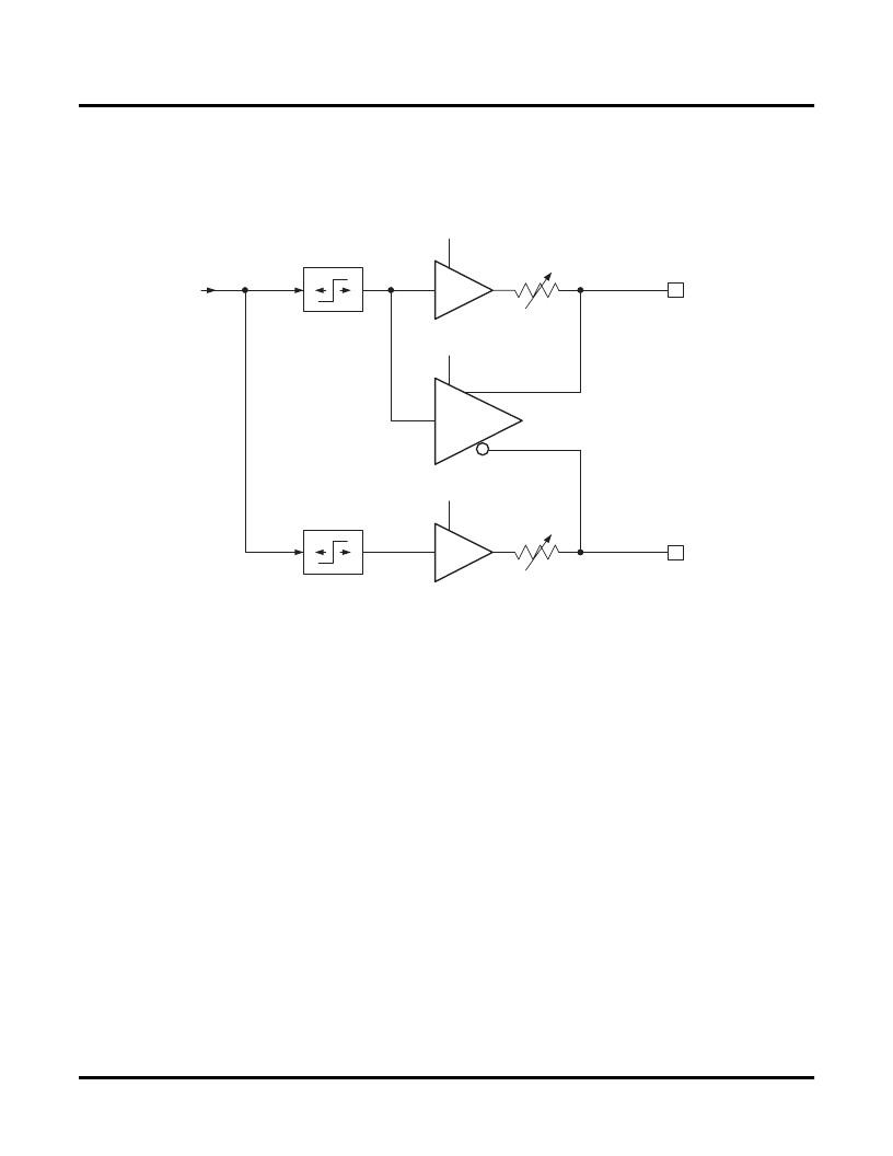
In the case where an output bank is unused, the associated VCCO pin may be either left
fl
oating or tied to ground
to reduce quiescent power consumption. We recommend, however, that all unused VCCO pins be tied to ground
where possible. All GND0 pins must be tied to ground, regardless of whether or not the associated bank is used.
Figure 19. ispClock5600 Output Driver and Skew Control
Each of the ispClock5600’s output driver banks can be con
fi
gured to support the following logic outputs:
LVTTL
LVCMOS (1.8V, 2.5V, 3.3V)
SSTL2
SSTL3
HSTL
LVDS
Differential LVPECL (3.3V)
To provide LVTTL, LVCMOS, SSTL2, SSTL3, and HSTL outputs, the CMOS output drivers in each bank are
enabled. These circuits provide logic outputs which swing from ground to the VCCO supply rail. The choice of
VCCO to be supplied to a given bank is determined by the logic standard to which that bank is con
fi
gured. Because
each pair of outputs has its own VCCO supply pin, each bank can be independently con
fi
gured to support a differ-
ent logic standard. Note that the two outputs associated with a bank must necessarily be con
fi
gured to the same
logic standard. The source impedance of each of the two outputs in each bank may be independently set over a
range of 40
to 70
in 5
steps. A low impedance option (
≈
20
) is also provided for cases where low source ter-
mination is desired on a given output.
Control of output slew rate is also provided in LVTTL, LVCMOS, SSTL2, SSTL3, and HSTL output modes. Four
output slew-rate settings are provided, as speci
fi
ed in the “Output Rise Times” and “Output Fall Times” tables in this
data sheet.
To provide LVDS and differential LVPECL outputs, a separate internal driver is used which provides the correct
LVDS or LVPECL logic levels when operating from a 3.3V VCCO. Because both LVDS and differential LVPECL
transmission lines are normally terminated with a single 100
resistor between the ‘+’ and ‘-’ signal lines at the far
OE
Control
From V-Dividers
Skew
Adjust
Skew
Adjust
BANKxA
BANKxB
Single-ended
‘A’ output Driver
Single-ended
‘B’ output Driver
Differential
(PECL/LVDS)
Driver
OE
Control
OE
Control
相關(guān)PDF資料 |
PDF描述 |
|---|---|
| ISPPAC-CLK5610V-01TN48C | LED Ring Light; LED Color:Infrared; Leaded Process Compatible:No; Peak Reflow Compatible (260 C):No; Supply Current:350mA; Supply Voltage:24VDC; Wavelength:880nm |
| ISPPAC-CLK5620V-01TN48C | LED Area Light; LED Color:Red; Leaded Process Compatible:No; Light Emitting Area:62x62mm; Peak Reflow Compatible (260 C):No; Supply Current:200mA; Supply Voltage:24VDC; Wavelength:630nm |
| ISPPAC-CLK5610V-01TN48I | Backlight LED; Color:Red; Digit/Alpha Height:70mm; Forward Current:250mA; Operating Temperature Range:0 C to +50 C; Leaded Process Compatible:No; Light Emitting Area:70x70mm; Peak Reflow Compatible (260 C):No; Supply Current:250mA |
| ISPPAC-CLK5620V-01TN48I | Backlight LED; Color:Red; Digit/Alpha Height:85mm; Forward Current:500mA; Operating Temperature Range:0 C to +50 C; Leaded Process Compatible:No; Light Emitting Area:85x220mm; Peak Reflow Compatible (260 C):No |
| ISPPAC-POWR1014 | In-System Programmable Power Supply Supervisor, Reset Generator and Sequencing Controller |
相關(guān)代理商/技術(shù)參數(shù) |
參數(shù)描述 |
|---|---|
| ISPPAC-CLK5620V-01TN48C | 制造商:LATTICE 制造商全稱(chēng):Lattice Semiconductor 功能描述:In-System Programmable, Zero-Delay Clock Generator with Universal Fan-Out Buffer |
| ISPPAC-CLK5620V-01TN48I | 制造商:LATTICE 制造商全稱(chēng):Lattice Semiconductor 功能描述:In-System Programmable, Zero-Delay Clock Generator with Universal Fan-Out Buffer |
| ISPPAC-POWR1014 | 制造商:LATTICE 制造商全稱(chēng):Lattice Semiconductor 功能描述:In-System Programmable Power Supply Supervisor, Reset Generator and Sequencing Controller |
| ISPPAC-POWR1014_08 | 制造商:LATTICE 制造商全稱(chēng):Lattice Semiconductor 功能描述:In-System Programmable Power Supply Supervisor, Reset Generator and Sequencing Controller |
| ispPAC-POWR1014-01T48I | 功能描述:監(jiān)控電路 Prec. Prog. Pwr Sppl y Seq. Mon. Trim I RoHS:否 制造商:STMicroelectronics 監(jiān)測(cè)電壓數(shù): 監(jiān)測(cè)電壓: 欠電壓閾值: 過(guò)電壓閾值: 輸出類(lèi)型:Active Low, Open Drain 人工復(fù)位:Resettable 監(jiān)視器:No Watchdog 電池備用開(kāi)關(guān):No Backup 上電復(fù)位延遲(典型值):10 s 電源電壓-最大:5.5 V 最大工作溫度:+ 85 C 安裝風(fēng)格:SMD/SMT 封裝 / 箱體:UDFN-6 封裝:Reel |
發(fā)布緊急采購(gòu),3分鐘左右您將得到回復(fù)。