- 您現(xiàn)在的位置:買(mǎi)賣(mài)IC網(wǎng) > PDF目錄65600 > IMIB9847BY (CYPRESS SEMICONDUCTOR CORP) LOW SKEW CLOCK DRIVER, 12 TRUE OUTPUT(S), 12 INVERTED OUTPUT(S), PDSO48 PDF資料下載
參數(shù)資料
| 型號(hào): | IMIB9847BY |
| 廠商: | CYPRESS SEMICONDUCTOR CORP |
| 元件分類(lèi): | 時(shí)鐘及定時(shí) |
| 英文描述: | LOW SKEW CLOCK DRIVER, 12 TRUE OUTPUT(S), 12 INVERTED OUTPUT(S), PDSO48 |
| 封裝: | SSOP-48 |
| 文件頁(yè)數(shù): | 4/7頁(yè) |
| 文件大?。?/td> | 64K |
| 代理商: | IMIB9847BY |
B9847
Document #: 38-07197 Rev. **
Page 4 of 7
Maximum Ratings
Input Voltage Relative to VSS:...............................VSS – 0.3V
Input Voltage Relative to VDD: ............................. VDD + 0.3V
Storage Temperature: ................................. –65
°C to +150°C
Operating Temperature: .................................... 0
°C to +70°C
Maximum Power Supply: ................................................5.5V
This device contains circuitry to protect the inputs against
damage due to high static voltages or electric field; however,
precautions should be taken to avoid application of any volt-
age higher than the maximum rated voltages to this circuit. For
proper operation, Vin and Vout should be constrained to the
range:
VSS < (Vin or Vout) < VDD
Unused inputs must always be tied to an appropriate logic volt-
age level (either VSS or VDD).
Notes:
2.
Unused inputs must be held high or low to prevent them from floating.
3.
Differential input signal voltage specifies the differential voltage |VTR – VCP| required for switching, where VTR is the true input level and VCP is the comple-
mentary input level. See Figure 1.
4.
Differential cross-point input voltage is expected to track VDD and is the voltage at which the differential signals must be crossing.
5.
For load conditions see Figure 1.
6.
The value of VOC is expected to be |VTR + VCP|/2. In case of each clock directly terminated by a 120
resistor. See Figure 1.
7.
All outputs switching loaded with 16 pF in 60
environment. See Figure 1.
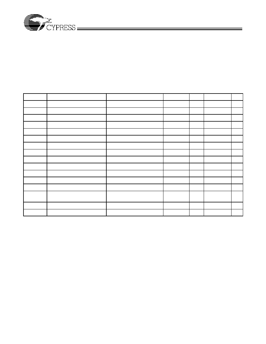
DC Parameters[2]: VDD2.5 = 2.5V + 5%, VDD3.3_2.5 = 3.3V + 5% or 2.5V + 5%, TA = 0°C to +70°C
Parameter
Description
Conditions
Min.
Typ.
Max.
Unit
VIL
Input Low Voltage
SDATA, SCLK
-
1.0
V
VIH
Input High Voltage
2.2
-
V
VIL1
Input Low Voltage
BUFIN, PD#
1.0
VIH1
Input High Voltage
2.0
IIH
Input High Current
VIN = VDD, BUFIN, PD#
10
A
IIL
Input Low Current
TBD
A
IOL
Output Low Current
VDD = 2.375V, VOUT = 1.2V
26
35
mA
IOH
Output High Current
VDD = 2.375V, VOUT = 1V
–18
-32
mA
VOL
Output Low Voltage
VDD = 2.375V, IOL = 12 mA
0.6
V
VOH
Output High Voltage
VDD = 2.375V, IOH = –12 mA
1.7
V
VOUT
Output Voltage Swing[5]
0.7
VDD+0.6
V
VOX
Output Crossing Voltage[6]
(VDD/2) – 0.2 VDD/2
(VDD/2) + 0.2
V
IOZ
High-Impedance Output Current
VO = GND or VO=VDD
–10
10
A
IDD
Dynamic Supply Current[7]
DDR mode, VDD = 2.65 volts,
FO = 133 MHz
187
210
mA
IDDS
Shutdown Supply Current
All VDD
mA
Cin
Input Pin Capacitance
5
-
pF
相關(guān)PDF資料 |
PDF描述 |
|---|---|
| IMICB664EYB | LOW SKEW CLOCK DRIVER, PDSO16 |
| IMISC401PB | 88 MHz, PROC SPECIFIC CLOCK GENERATOR, PDIP20 |
| IMISC414YB | 80 MHz, PROC SPECIFIC CLOCK GENERATOR, PDSO24 |
| IMISC417PB | 88 MHz, PROC SPECIFIC CLOCK GENERATOR, PDIP20 |
| IMISC451XB | 40 MHz, OTHER CLOCK GENERATOR, PDSO16 |
相關(guān)代理商/技術(shù)參數(shù) |
參數(shù)描述 |
|---|---|
| IMIB9940 | 制造商:未知廠家 制造商全稱(chēng):未知廠家 功能描述:Clocks and Buffers |
| IMIB9940LBL | 制造商:Cypress Semiconductor 功能描述:Clock Driver 2-IN 32-Pin TQFP 制造商:Rochester Electronics LLC 功能描述:CLOCK BUFFER.18 OUTPUTS, 200MHZ, 2.5V . - Bulk |
| IMIB9940LBLT | 制造商:CYPRESS 制造商全稱(chēng):Cypress Semiconductor 功能描述:2.5V or 3.3V, 200-MHz, 1:18 Clock Distribution Buffer |
| IMIB9946 | 制造商:未知廠家 制造商全稱(chēng):未知廠家 功能描述:Clocks and Buffers |
| IMIB9946CA | 制造商:Cypress Semiconductor 功能描述:Logic ICS, 3.3V, 160MHz, 1:10 Clock Distribution Buffer 制造商:Rochester Electronics LLC 功能描述:CLOCK BUFFER.18 OUTPUTS, 160MHZ, 3.3V . - Bulk |
發(fā)布緊急采購(gòu),3分鐘左右您將得到回復(fù)。