- 您現(xiàn)在的位置:買賣IC網(wǎng) > PDF目錄385403 > HT82J97E (Holtek Semiconductor Inc.) USB Joystick Encoder 8-Bit OTP MCU PDF資料下載
參數(shù)資料
| 型號: | HT82J97E |
| 廠商: | Holtek Semiconductor Inc. |
| 英文描述: | USB Joystick Encoder 8-Bit OTP MCU |
| 中文描述: | USB搖桿編碼器8位微控制器檢察官辦公室 |
| 文件頁數(shù): | 25/46頁 |
| 文件大小: | 314K |
| 代理商: | HT82J97E |
第1頁第2頁第3頁第4頁第5頁第6頁第7頁第8頁第9頁第10頁第11頁第12頁第13頁第14頁第15頁第16頁第17頁第18頁第19頁第20頁第21頁第22頁第23頁第24頁當(dāng)前第25頁第26頁第27頁第28頁第29頁第30頁第31頁第32頁第33頁第34頁第35頁第36頁第37頁第38頁第39頁第40頁第41頁第42頁第43頁第44頁第45頁第46頁
HT82J97E
Rev. 1.30
25
May 10, 2004
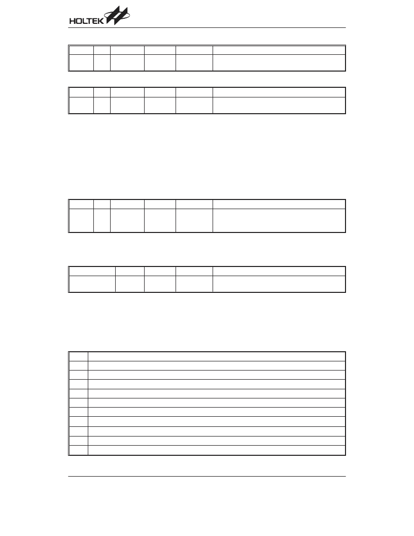
ADC High-byte Data Register ADCR (Address 0X1E)
Register Bits
Labels
Read/Write
Option
Functions
ADCR
(0X1E)
7~0
PG7~PG0
R
ADCDR
TheADCDRstorestheresultofavalidADCconversion
bit7~bit0.
Table High Byte Pointer for Current Table Read TBHP(Address 0X1F)
Register Bits
Labels
Read/Write
Option
Functions
TBHP
(0X1F)
2~0
PGC2~PG0
R
Store current table read bit10~bit8 data
PWM Base Period Register PWMBR (Address 0X18)
Thisregisterisusedtodefinethebaseperiod ofthePWMcycleperiod.Theperiodisdefinedaccordingtothefollowing
equation:
Base period = (4/f
SYS
) (PWMBR+1) or (1/f
SYS
)
(PWMBR+1)
Where 4/f
SYS
or 1/f
SYS
is defined by PWM_S bit of PORT_PC
Where PWMBR = 1~255, PWMBR=0 is not available
PWMcycle period = 256 Base period
Base period equals to 1/256 duty cycle.
Register Bits
Labels
Read/Write
Option
Functions
PWMBR
(0X18)
7~0
PD7~PD0
R
Used to define the base period of the PWM
Range =2~256 Base Period
Where PWMBR=1~255, PWMBR=0 is not available
PWM Duty Register PWM1DR (Address 0XCH) and PWM2DR (Address 0XDH)
This register is used to define the duty of the PWM1 output (PC2) or PWM2 output (PC3) respectively. Both PWM cycle
frequency is defined according to the following equation:
Register
Bits
Read/Write
Option
Functions
PWM1DR (0XCH)
PWM2DR (0XDH)
7~0
R/W
Used to define the PWM duty
PWM1 duty = (PWM1DR+1)/PWM cycle 100% period
Where PWM1DR= 0~255
If the PWM function is enabled by setting the corresponding bit (PWM1_EN or PWM2_EN of Port C), the PWM output
(PC2 or PC3) pins always output the PWM signal whether the corresponding control register bit (PCC2 or PCC3 ) is de-
fined as in input or output mode.
OTP Options
No.
Option
1
WDT clock source: RC (system/4) (default: T1)
2
WDT clock source: enable/disable for normal mode (default: disable)
3
PA0~PA7,PB4,PB7wake-upbybit(PA2,PA3bothwake-upbyfallingorrisingedge)(default:nonwake-up)
4
PA0~PA7 pull-high by bit (default: Pull-high)
5
PC0~3,PB pull-high by nibble (default: Pull-high)
6
2.7 V (error 0.3V) LVR enable/disable (default: enable)
7
PA0~PA3, PB2, PB3 Pull-low by bit (default: non pull-low 30k )
8
CLR WDT , 1 or 2 instructions
9
TBHP enable/disable (default: disable)
10
PA output mode (CMOS/NMOS/PMOS) by bit (default: CMOS)
The LVR voltage is define as 2.7V 0.3V and default is enable.
相關(guān)PDF資料 |
PDF描述 |
|---|---|
| HT82J97E-20SOP-A | USB Joystick Encoder 8-Bit OTP MCU |
| HT82J97E-28SOP-A | USB Joystick Encoder 8-Bit OTP MCU |
| HT82K28 | Win98 Keyboard Encoder |
| HT82K28A | Win98 Keyboard Encoder |
| HT82K628A | Windows 2000 Keyboard Encoder(Windows 2000操作系統(tǒng)鍵盤編碼器) |
相關(guān)代理商/技術(shù)參數(shù) |
參數(shù)描述 |
|---|---|
| HT82J97E_08 | 制造商:HOLTEK 制造商全稱:Holtek Semiconductor Inc 功能描述:USB Joystick Encoder 8-Bit MCU |
| HT82J97E-20SOP-A | 制造商:HOLTEK 制造商全稱:Holtek Semiconductor Inc 功能描述:USB Joystick Encoder 8-Bit OTP MCU |
| HT82J97E-28SOP-A | 制造商:HOLTEK 制造商全稱:Holtek Semiconductor Inc 功能描述:USB Joystick Encoder 8-Bit OTP MCU |
| HT82K19 | 制造商:未知廠家 制造商全稱:未知廠家 功能描述:Peripheral IC |
| HT82K28 | 制造商:HOLTEK 制造商全稱:Holtek Semiconductor Inc 功能描述:Win98 Keyboard Encoder |
發(fā)布緊急采購,3分鐘左右您將得到回復(fù)。