- 您現(xiàn)在的位置:買賣IC網(wǎng) > PDF目錄385403 > HT82J97E (Holtek Semiconductor Inc.) USB Joystick Encoder 8-Bit OTP MCU PDF資料下載
參數(shù)資料
| 型號(hào): | HT82J97E |
| 廠商: | Holtek Semiconductor Inc. |
| 英文描述: | USB Joystick Encoder 8-Bit OTP MCU |
| 中文描述: | USB搖桿編碼器8位微控制器檢察官辦公室 |
| 文件頁數(shù): | 20/46頁 |
| 文件大?。?/td> | 314K |
| 代理商: | HT82J97E |
第1頁第2頁第3頁第4頁第5頁第6頁第7頁第8頁第9頁第10頁第11頁第12頁第13頁第14頁第15頁第16頁第17頁第18頁第19頁當(dāng)前第20頁第21頁第22頁第23頁第24頁第25頁第26頁第27頁第28頁第29頁第30頁第31頁第32頁第33頁第34頁第35頁第36頁第37頁第38頁第39頁第40頁第41頁第42頁第43頁第44頁第45頁第46頁

HT82J97E
Rev. 1.30
20
May 10, 2004
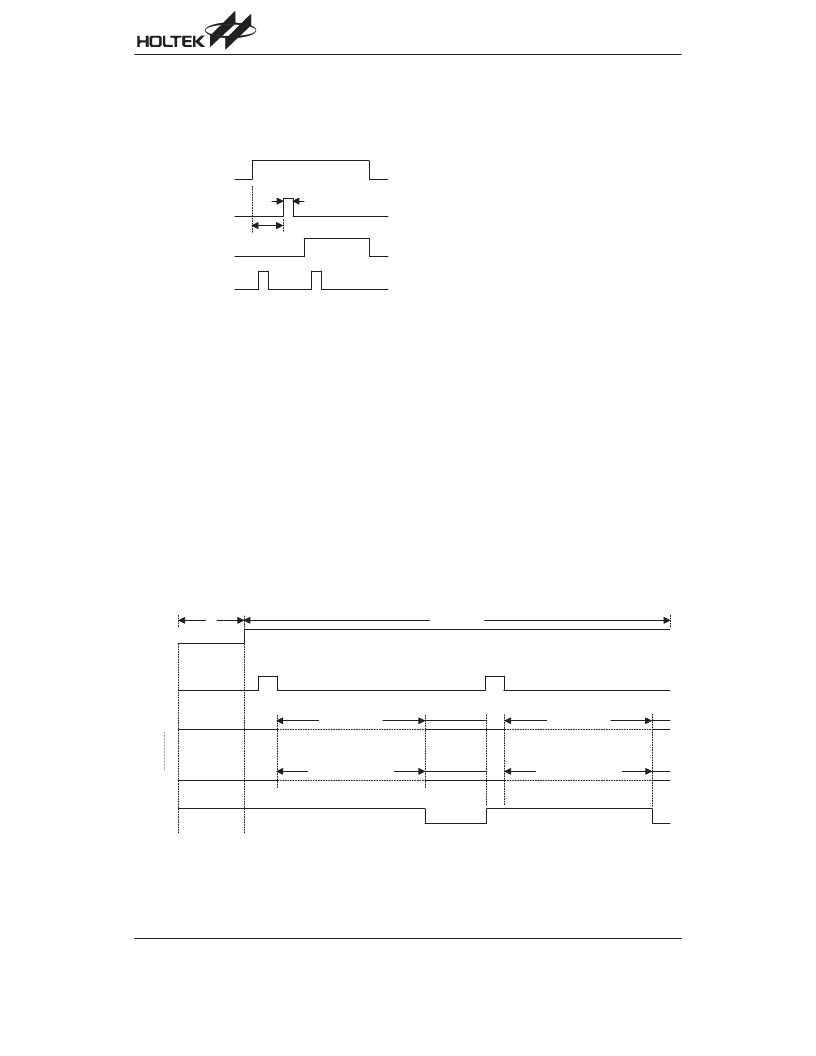
The device with remote wake-up function can wake-up
the USB Host by sending a wake-up pulse through
RMWK (bit 1 of USC). Once the USB Host receive the
wake-up signal from the HT82J97E, it will send a Re-
sume signal to the device. The timing is as follows:
To Configure the HT82J97E as PS2 Device
The HT82J97E can be defined as a USB interface or a
PS2 interface by configuring the SPS2 (bit 4 of the USR)
and SUSB (bit 5 of the USR). If SPS2=1, and SUSB=0,
the HT82J97E is defined as PS2 interface, pin USBD- is
now defined as PS2 Data pin and USBD+ is now de-
fined as PS2 Clk pin. The user can easily read or write to
the PS2 Data or PS2 Clk pin by accessing the corre-
sponding bit PS2DAI (bit 4 of the USC), PS2CKI (bit 5 of
the USC), PS2DAO (bit 6 of the USC) and S2CKO (bit 7
of the USC) respectively.
The user should make sure that in order to read the data
properly, the corresponding output bit must be set to 1 .
For example, if user wants to read the PS2 Data by
reading PS2DAI, the PS2DAO should be set to 1 . Oth-
erwise it always read a 0 .
If SPS2=0, and SUSB=1, the HT82J97E is defined as a
USB interface. Both the USBD- and USBD+ are driven
by the USB SIE of the HT82J97E. User only writes or
reads the USB data through the corresponding FIFO.
Both SPS2 and SUSB default is 0 .
To Configure the ADC Block
The HT82J97E has built-in an 8-bit A/D converter with 6
channels (PB0~PB5). In order to make the A/D con-
verter more flexible, there are two modes: External Ref-
erence voltage and Internal Reference voltage. It can be
easily configured by setting the ADREF (bit 6 of the
USR). For External Reference voltage, the reference
voltage of the A/D converter comes from an external
PB6/VRL and PB7/VRH pins. Otherwise, the reference
voltage is coming from the VDD and VSS of the MCU.
PB0~PB5 is the 6-channel input of the A/D converter, it
is easy to define which channel is converting by config-
uring ACS2~ACS0 (bit 2~0 of the ADSC). Also there are
four converter clock sources to be selected by setting
ADCS1(bit4oftheADSC),ADCS0(bit3oftheADSC).
Once the ADON (bit 6 of the ADSC) is set, it sends the
start pulse through START (bit 5 of ADSC). The A/D
converter will be in operation. There are EOCB (bit 7 of
the ADSC) to indicate whether the A/D converter is busy
or not. The EOCB is cleared when the conversion is
completed. User can read the converter data by reading
the register ADR. In order to meet 500 A suspend cur-
rent spec., user should disable the A/D by clearing
ADON before jumping to suspend mode.
- (
!
(
,
- B
+
4 4 /
!
4 ( (
- (
#
The following is an A/D converter timing diagram:
, (
"
)
(
3
!
(
!
)
(
3
!
(
!
)
(
3
!
)
(
3
!
(
)
(
3
!
( :
! $
"
C
B "
C
)
(
3
!
( :
! $
"
(
(
(
(
)
(
3
!
)
(
3
!
(
(
(
(
(
1
-
相關(guān)PDF資料 |
PDF描述 |
|---|---|
| HT82J97E-20SOP-A | USB Joystick Encoder 8-Bit OTP MCU |
| HT82J97E-28SOP-A | USB Joystick Encoder 8-Bit OTP MCU |
| HT82K28 | Win98 Keyboard Encoder |
| HT82K28A | Win98 Keyboard Encoder |
| HT82K628A | Windows 2000 Keyboard Encoder(Windows 2000操作系統(tǒng)鍵盤編碼器) |
相關(guān)代理商/技術(shù)參數(shù) |
參數(shù)描述 |
|---|---|
| HT82J97E_08 | 制造商:HOLTEK 制造商全稱:Holtek Semiconductor Inc 功能描述:USB Joystick Encoder 8-Bit MCU |
| HT82J97E-20SOP-A | 制造商:HOLTEK 制造商全稱:Holtek Semiconductor Inc 功能描述:USB Joystick Encoder 8-Bit OTP MCU |
| HT82J97E-28SOP-A | 制造商:HOLTEK 制造商全稱:Holtek Semiconductor Inc 功能描述:USB Joystick Encoder 8-Bit OTP MCU |
| HT82K19 | 制造商:未知廠家 制造商全稱:未知廠家 功能描述:Peripheral IC |
| HT82K28 | 制造商:HOLTEK 制造商全稱:Holtek Semiconductor Inc 功能描述:Win98 Keyboard Encoder |
發(fā)布緊急采購,3分鐘左右您將得到回復(fù)。