- 您現(xiàn)在的位置:買賣IC網(wǎng) > PDF目錄384423 > HIP7010 (Intersil Corporation) J1850 Byte Level Interface Circuit PDF資料下載
參數(shù)資料
| 型號: | HIP7010 |
| 廠商: | Intersil Corporation |
| 英文描述: | J1850 Byte Level Interface Circuit |
| 中文描述: | J1850字節(jié)級接口電路 |
| 文件頁數(shù): | 5/20頁 |
| 文件大小: | 106K |
| 代理商: | HIP7010 |
5
Functional Pin Description
This section provides a description of each of the 14 pins of
the HIP7010 as shown in Figure 2.
V
DD
and V
SS
(Power)
Power is supplied to the HIP7010 using these two pins. V
DD
is connected to the positive supply and V
SS
is connected to
the negative supply.
CLK (Clock - Input)
The Clock input (CLK) provides the basic time base refer-
ence for all J1850 symbol detection and generation. Serial
Bus transfers between the HIP7010 and the Host microcon-
troller are also timed based on the Clock input. Proper VPW
symbol detection and generation requires a 2MHz clock
which is internally derived from the CLK input. Various CLK
input frequencies can be accommodated via the Divide
Select bits in the Status/Control Register (see
Status/Con-
trol Register
for details).
An internal Slow Clock Detect circuit monitors the CLK input
signal and generates a HIP7010 reset if the clock is inactive
for more than
1/f
SLOW
. This is a safety mechanism to prevent
blocking the J1850 and Serial busses in the event of a clock
failure. The Slow Clock Detect reset can also be intentionally
invoked by externally inhibiting CLK input transitions.
Power can be reduced under Host control via the PowerDown
bit in the Status/Control Register (see Status/Control Regis-
ter for details). Setting the Power-Down bit effectively stops
internal clocking of the HIP7010.
(OUTPUT)
SCK
(OUTPUT)
SIN
(INPUT)
SOUT
(OUTPUT)
D7I
D6I
D0I
D7O
D6O
D0O
(6)
(11)
(8)
(5)
(12)
(13)
(1)
(4)
(7)
SACTIVE
(INPUT)
RDY (LONG)
(INPUT)
RDY (SHORT)
STAT
(INPUT)
(2)
(10)
(9)
(3)
(14)
(15)
(16)
(17)
(18)
(19)
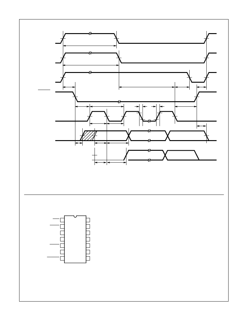
FIGURE 1. SERIAL INTERFACE TIMING DIAGRAM
NOTES:
1. Measurement points are from V
DD
/2, except 12 and 13 which are measured between V
IL
and V
IH.
2. All timings assume proper CLK frequency and Divide Select values to generate 1MHz SCK.
IDLE
VPWIN
VPWOUT
V
DD
RESET
TEST
SACTIVE
RDY
STAT
CLK
V
SS
SIN
SOUT
SCK
1
2
3
4
5
6
7
14
13
12
11
10
9
8
FIGURE 2. 14 PIN DIP AND SO TERMINAL ASSIGNMENTS
HIP7010
相關(guān)PDF資料 |
PDF描述 |
|---|---|
| HIP7010B | J1850 Byte Level Interface Circuit |
| HIP7010P | FPGA 2000000 SYSTEM GATE 1.8 VOLT - NOT RECOMMENDED for NEW DESIGN |
| HIP7020 | FPGA 2000000 SYSTEM GATE 1.8 VOLT - NOT RECOMMENDED for NEW DESIGN |
| HIP7020AB | FPGA 2000000 SYSTEM GATE 1.8 VOLT - NOT RECOMMENDED for NEW DESIGN |
| HIP7020AP | FPGA 2000000 SYSTEM GATE 1.8 VOLT - NOT RECOMMENDED for NEW DESIGN |
相關(guān)代理商/技術(shù)參數(shù) |
參數(shù)描述 |
|---|---|
| HIP7010B | 制造商:INTERSIL 制造商全稱:Intersil Corporation 功能描述:J1850 Byte Level Interface Circuit |
| HIP7010P | 制造商:Rochester Electronics LLC 功能描述:J1850 JBLIC (DIP) - Bulk |
| HIP7010P WAF | 制造商:Harris Corporation 功能描述: |
| HIP7020 | 制造商:INTERSIL 制造商全稱:Intersil Corporation 功能描述:J1850 Bus Transceiver For Multiplex Wiring Systems |
| HIP7020 DIE | 制造商:Harris Corporation 功能描述: |
發(fā)布緊急采購,3分鐘左右您將得到回復(fù)。