- 您現(xiàn)在的位置:買賣IC網(wǎng) > PDF目錄384423 > HIP7010 (Intersil Corporation) J1850 Byte Level Interface Circuit PDF資料下載
參數(shù)資料
| 型號: | HIP7010 |
| 廠商: | Intersil Corporation |
| 英文描述: | J1850 Byte Level Interface Circuit |
| 中文描述: | J1850字節(jié)級接口電路 |
| 文件頁數(shù): | 10/20頁 |
| 文件大?。?/td> | 106K |
| 代理商: | HIP7010 |
10
block. The STATE block controls the flow of all data between
the SERIAL and SENDEC blocks. The STATE block also con-
trols Host/HIP7010 handshaking, automatic J1850 bus arbi-
tration, break recognition, CRC checking, and many other
features. In addition to the three major blocks the HIP7010
includes CRC generator/checker hardware, a Status/Control
Register, and a Timing generator.
Timing Generator
The timing generator, as its name suggests, generates all
internal timing pulses required for the SERIAL, SENDEC,
STATE, and CRC circuits. The CLK input pin is appropriately
divided to produce an internal 2MHz clock which results in a
1MHz SERIAL transfer rate and VPW J1850 symbol timing
with 1
μ
s accuracy. The CLK pin of the HIP7010 can be driven
with a variety of common microcontroller frequencies. Fre-
quency selection is accomplished via three bits in the Sta-
tus/Control register. See
Status/Control Register
for more
details.
The Serial Interface (SERIAL) System
Overview
The SERIAL system handles all interface between the Host
microcontroller and the HIP7010. The SERIAL system is
designed to interface directly with the Serial Peripheral Inter-
face (SPI) systems of the Intersil CDP68HC05 family of micro-
controllers. Identical interfaces are found on the 68HC11 and
HC16 families. Compatible systems are found on most popu-
lar microcontrollers.
Serial data words are simultaneously transmitted and
received over the SOUT/SIN lines, synchronized to the SCK
clock stream. The word size is fixed at 8-bits. A series of
eight clocks is required to transfer one word. With the excep-
tion of Status/Control Register transfers (described later), all
SERIAL transfers use a single eight bit shift register within
the HIP7010. The serial bits are “shifted out” on the SOUT
pin, most significant bit (MSB) first, from the shift register. As
each bit shifts out one end of the shift register, the data on
the SIN input pin is, usually, shifted into the other end of the
same shift register. After eight clocks, the original contents of
the shift register have been entirely transmitted on the SOUT
pin and replaced by the byte received on the SIN pin.
Most Host micros which include a synchronous serial inter-
face, operate their interface in a manner compatible with the
HIP7010s implementation. The result of each 8-bit SERIAL
transfer is that the contents of the HIP7010s shift register
and the Host’s shift register have effectively been “swapped”.
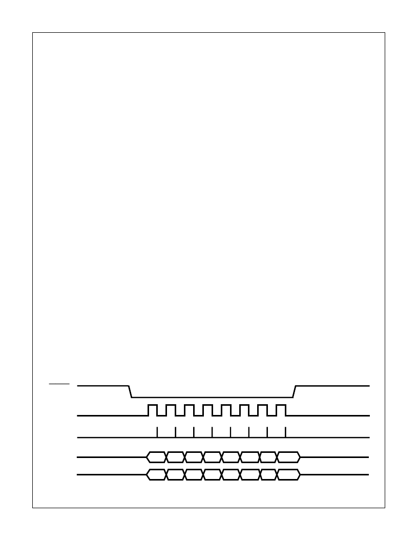
SERIAL Bus Timing
The SCK output of the HIP7010 is used to synchronize the
movement of data both into and out of the device on its SIN
and SOUT lines. As stated above, the Host and the HIP7010
are capable of exchanging a byte of information during a
sequence of eight clocks generated on the SCK pin. The
relationship between the clock signal on SCK and the data
on SIN and SOUT is shown in Figure 7.
At least t
LEAD
prior to each series of eight clocks, the SAC-
TIVE output of the HIP7010 is driven low. SACTIVE remains
low until a minimum of
t
LAG
after the last clock transition.
When interfacing to a CDP68HC05 SPI compatible Host, the
SACTIVE output would normally be connected to the SS input
of the Host. The trailing edge of the SACTIVE signal can also
be used as a flag to Hosts which don’t automatically recognize
the transfer of a serial byte.
The quiescent state of SCK is low. Once a transfer is initi-
ated, the rising edge of each SCK pulse places the next bit
on the SOUT line and the falling edge is used to latch the bit
input on SIN.
The Host must adhere to this same timing, by meeting the input
setup time requirements of SIN valid before the trailing edge of
SCK (see
Electrical Specification
for details) and latching
the SOUT data on the same edge. When interfacing the
HIP7010 to a CDP68HC05 SPI compatible Host, the SPI inter-
face should be programmed with CPHA = 1 and CPOL = 0.
At all times, other than during an actual SERIAL transfer
between the HIP7010 and its Host, the SCK and SOUT pins
are held in a high impedance state. This allows other devices
connected to the Host via the SERIAL bus to be accessed
when the HIP7010 is not transferring data. Utilization of the
SERIAL bus by the HIP7010 is less than 5%, leaving signifi-
cant bandwidth for other transfers. When held in the high
impedance state, a pair of integrated pull-down devices on the
SCK and SOUT pull the pins to ground, if they are not driven
by another source. See
Applications Information
for a
detailed discussion of SERIAL bus utilization.
SCK
SOUT
SIN
SACTIVE
SCKNORMALLY LOW
MSB
MSB
6
6
5
5
4
4
3
3
2
2
1
1
LSB
LSB
INTERNAL STROBE FORLATCHING DATA INHIP7010
MSB
6
5
4
3
2
1
LSB
FIGURE 7. SERIAL BUS TIMING
HIP7010
相關(guān)PDF資料 |
PDF描述 |
|---|---|
| HIP7010B | J1850 Byte Level Interface Circuit |
| HIP7010P | FPGA 2000000 SYSTEM GATE 1.8 VOLT - NOT RECOMMENDED for NEW DESIGN |
| HIP7020 | FPGA 2000000 SYSTEM GATE 1.8 VOLT - NOT RECOMMENDED for NEW DESIGN |
| HIP7020AB | FPGA 2000000 SYSTEM GATE 1.8 VOLT - NOT RECOMMENDED for NEW DESIGN |
| HIP7020AP | FPGA 2000000 SYSTEM GATE 1.8 VOLT - NOT RECOMMENDED for NEW DESIGN |
相關(guān)代理商/技術(shù)參數(shù) |
參數(shù)描述 |
|---|---|
| HIP7010B | 制造商:INTERSIL 制造商全稱:Intersil Corporation 功能描述:J1850 Byte Level Interface Circuit |
| HIP7010P | 制造商:Rochester Electronics LLC 功能描述:J1850 JBLIC (DIP) - Bulk |
| HIP7010P WAF | 制造商:Harris Corporation 功能描述: |
| HIP7020 | 制造商:INTERSIL 制造商全稱:Intersil Corporation 功能描述:J1850 Bus Transceiver For Multiplex Wiring Systems |
| HIP7020 DIE | 制造商:Harris Corporation 功能描述: |
發(fā)布緊急采購,3分鐘左右您將得到回復(fù)。