- 您現(xiàn)在的位置:買賣IC網(wǎng) > PDF目錄370311 > GCIXP1250-232 Microprocessor PDF資料下載
參數(shù)資料
| 型號: | GCIXP1250-232 |
| 英文描述: | Microprocessor |
| 中文描述: | 微處理器 |
| 文件頁數(shù): | 138/148頁 |
| 文件大?。?/td> | 1601K |
| 代理商: | GCIXP1250-232 |
第1頁第2頁第3頁第4頁第5頁第6頁第7頁第8頁第9頁第10頁第11頁第12頁第13頁第14頁第15頁第16頁第17頁第18頁第19頁第20頁第21頁第22頁第23頁第24頁第25頁第26頁第27頁第28頁第29頁第30頁第31頁第32頁第33頁第34頁第35頁第36頁第37頁第38頁第39頁第40頁第41頁第42頁第43頁第44頁第45頁第46頁第47頁第48頁第49頁第50頁第51頁第52頁第53頁第54頁第55頁第56頁第57頁第58頁第59頁第60頁第61頁第62頁第63頁第64頁第65頁第66頁第67頁第68頁第69頁第70頁第71頁第72頁第73頁第74頁第75頁第76頁第77頁第78頁第79頁第80頁第81頁第82頁第83頁第84頁第85頁第86頁第87頁第88頁第89頁第90頁第91頁第92頁第93頁第94頁第95頁第96頁第97頁第98頁第99頁第100頁第101頁第102頁第103頁第104頁第105頁第106頁第107頁第108頁第109頁第110頁第111頁第112頁第113頁第114頁第115頁第116頁第117頁第118頁第119頁第120頁第121頁第122頁第123頁第124頁第125頁第126頁第127頁第128頁第129頁第130頁第131頁第132頁第133頁第134頁第135頁第136頁第137頁當前第138頁第139頁第140頁第141頁第142頁第143頁第144頁第145頁第146頁第147頁第148頁
Intel
IXP1250 Network Processor
138
Datasheet
4.3.9.3
SDRAM Signal Protocol
This section describes the SDRAM timing parameters referenced in the SDRAM timing diagrams
that follow. This nomenclature is consistent with most JEDEC standard SDRAM devices.
tRP
tRP is the minimum number of cycles after a precharge cycle that a bank may be opened (or
"RASd"). The
IXP1200 Network Processor Family Micrcode Programmer
’
s Reference Manual
refers to this as the tRP Precharge Time. Also referred to as
“
PRECHARGE command period
”
in
SDRAM datasheets.
tRASmin
tRASmin is the minimum number of cycles that a bank must be open before it can be closed using
a precharge command. The maximum time that a bank may be open, tRASmax, is not checked,
because the IXP1250 SDRAM Controller methodology is to close all banks after the usage is
complete. The
IXP1200 Network Processor Family Micrcode Programmer
’
s Reference Manual
refers to this as the tRASmin Active Command Period. Also referred to as
“
ACTIVE to
PRECHARGE command period
”
in SDRAM datasheets.
tRCD
tRCD is the number of cycles between the bank opening (or "RAS") and any read or write
command (or "CAS"). The
IXP1200 Network Processor Family Micrcode Programmer
’
s
Reference Manual
refers to this as the tRCD RAS to CAS Delay. Also referred to as
“
ACTIVE to
READ or WRITE delay
”
in SDRAM datasheets.
tRRD
tRRD is the number of cycles between successive bank openings, or RAS cycles. The
IXP1200
Network Processor Family Micrcode Programmer
’
s Reference Manual
refers to this as the tRRD
Bank to Bank Delay Time. Also referred to as
“
ACTIVE bank A to ACTIVE bank B command
”
in
SDRAM datasheets.
tRC
tRC is the SDRAM bank cycle time, indicating that the minimum time that a command may be
active. For most cases, this is the sum of tRP and tRASmin, although there are some SDRAM data
sheets where the absolute time for tRC (in ns) is not equal to the sum (in ns) of tRP and tRASmin.
In these cases, typically when rounding up to an even number of clock cycles, they are equivalent.
Since the SDRAM Controller CSRs are programmed with a number of clock cycles, these
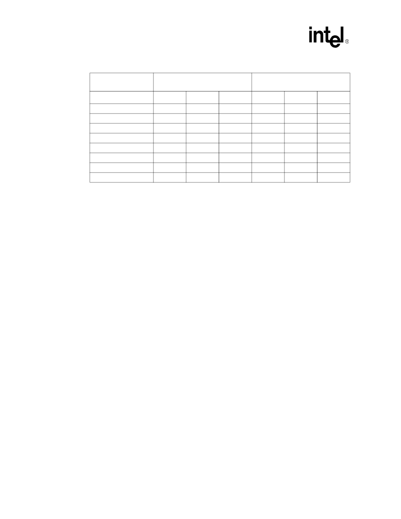
Table 52. Signal Delay Deratings for T
val
and T
ctl
Signal
Maximum Derating (ns/pF)
(IX Bus Speed)
Minimum Derating (ns/pF)
(IX Bus Speed)
83 MHz
100 MHz
116 MHz
83 MHz
100 MHz
116 MHz
SDCLK
0.053
—
—
0.025
—
—
DQM
0.065
0.06
0.031
0.03
0.025
0.015
WE_L
0.065
0.06
0.031
0.03
0.025
0.015
RAS_L
0.065
0.06
0.031
0.03
0.025
0.015
CAS_L
0.065
0.06
0.031
0.03
0.025
0.015
MADR[14:0]
0.065
0.06
0.031
0.03
0.025
0.015
MDATA[63:0]
0.095
0.09
0.035
0.03
0.025
0.015
MDATA_ECC[7:0]
0.095
0.09
0.035
0.03
0.025
0.015
相關PDF資料 |
PDF描述 |
|---|---|
| GCK101 | Analog IC |
| GCK131 | Microcontroller |
| GCM-3.15A | Fuse |
| GCM-4A | Fuse |
| GCM-5A | Fuse |
相關代理商/技術參數(shù) |
參數(shù)描述 |
|---|---|
| GCIXP1250BA | 功能描述:IC MPU NETWORK 166MHZ 520-BGA RoHS:否 類別:集成電路 (IC) >> 嵌入式 - 微處理器 系列:- 標準包裝:40 系列:MPC83xx 處理器類型:32-位 MPC83xx PowerQUICC II Pro 特點:- 速度:267MHz 電壓:0.95 V ~ 1.05 V 安裝類型:表面貼裝 封裝/外殼:516-BBGA 裸露焊盤 供應商設備封裝:516-PBGAPGE(27x27) 包裝:托盤 |
| GCIXP1250BB | 功能描述:IC MPU NETWORK 200MHZ 520-BGA RoHS:否 類別:集成電路 (IC) >> 嵌入式 - 微處理器 系列:- 標準包裝:40 系列:MPC83xx 處理器類型:32-位 MPC83xx PowerQUICC II Pro 特點:- 速度:267MHz 電壓:0.95 V ~ 1.05 V 安裝類型:表面貼裝 封裝/外殼:516-BBGA 裸露焊盤 供應商設備封裝:516-PBGAPGE(27x27) 包裝:托盤 |
| GCIXP1250BC | 功能描述:IC MPU NETWORK 232MHZ 520-BGA RoHS:否 類別:集成電路 (IC) >> 嵌入式 - 微處理器 系列:- 標準包裝:40 系列:MPC83xx 處理器類型:32-位 MPC83xx PowerQUICC II Pro 特點:- 速度:267MHz 電壓:0.95 V ~ 1.05 V 安裝類型:表面貼裝 封裝/外殼:516-BBGA 裸露焊盤 供應商設備封裝:516-PBGAPGE(27x27) 包裝:托盤 |
| GCJ0335C5C0JR50D | 制造商:MURATA 制造商全稱:Murata Manufacturing Co., Ltd. 功能描述:Chip Monolithic Ceramic Capacitors |
| GCJ0335C5C1AR50D | 制造商:MURATA 制造商全稱:Murata Manufacturing Co., Ltd. 功能描述:Chip Monolithic Ceramic Capacitors |
發(fā)布緊急采購,3分鐘左右您將得到回復。