- 您現(xiàn)在的位置:買賣IC網(wǎng) > PDF目錄1922 > FUSB1500MHX (Fairchild Semiconductor)IC USB 2.0 TRANSCEIVER 16-MLP PDF資料下載
參數(shù)資料
| 型號: | FUSB1500MHX |
| 廠商: | Fairchild Semiconductor |
| 文件頁數(shù): | 10/15頁 |
| 文件大小: | 0K |
| 描述: | IC USB 2.0 TRANSCEIVER 16-MLP |
| 標準包裝: | 3,000 |
| 類型: | USB 收發(fā)器 |
| 驅(qū)動器/接收器數(shù): | 1/1 |
| 規(guī)程: | USB 2.0 |
| 電源電壓: | 3 V ~ 3.6 V |
| 安裝類型: | 表面貼裝 |
| 封裝/外殼: | 16-WFQFN 裸露焊盤 |
| 供應商設備封裝: | 16-MLP(3x3) |
| 包裝: | 帶卷 (TR) |
2008 Fairchild Semiconductor Corporation
www.fairchildsemi.com
FUSB1500 Rev. 1.0.1
4
FUSB1500
/
FUSB1501
—
USB2.0
Full-Speed
/
Low-Speed
Transceiver
with
Charger
Detection
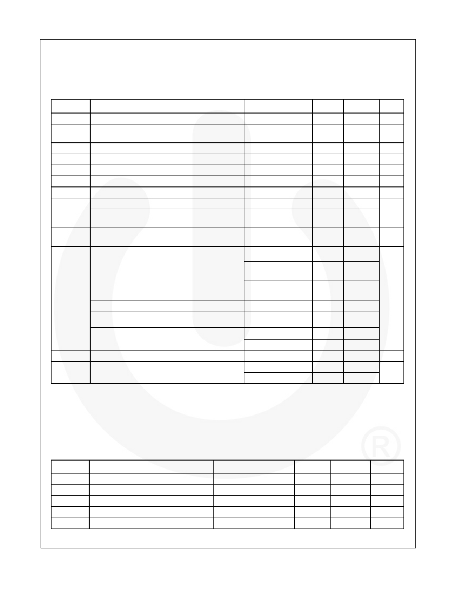
Absolute Maximum Ratings
Stresses exceeding the absolute maximum ratings may damage the device. The device may not function or be
operable above the recommended operating conditions and stressing the parts to these levels is not recommended.
In addition, extended exposure to stresses above the recommended operating conditions may affect device reliability.
The absolute maximum ratings are stress ratings only.
Symbol
Parameter
Test Conditions
Min.
Max.
Units
VIO
I/O Supply Voltage
-0.5
4.6
V
VPU,
VREG3V3
Regulated Supply Voltage and Pull-up Supply
-0.5
4.6
V
ILU
Latch-up Current
VIN = -1.8 to +5.4V
150
mA
IIK
DC Input Current
VIN < 0
-50
mA
VIN
DC Input Voltage
(1)
-0.5
VIO +0.5
V
IOK
DC Output Diode Current
VOUT > VREG3V3 or < 0
±50
mA
VOUT
DC Output Voltage
(1)
-0.5
VIO +0.5
V
IOUT
DC Output Source or Sink Current for D+, D- Pins
VOUT = 0 to VREG3V3
±50
mA
DC Output Source or Sink Current for RCV,
VM/VP
VOUT = 0 to VREG3V3
±15
IVREG3V3,
IGND
DC VVREG3V3 or GND Current
±100
mA
ESD
Human Body Model, JEDEC: JESD22-A114
Pins D+, D-, ILI < 3A
-10500
+10500
V
VREG3V3, VIO, and
GND; ILI < 3A;
-12000
+12000
All Other Pins,
ILI < 1A
-6500
+6500
Machine Model, JESD22-A115
200
Charged Device Model, JEDEC: JESD-C101
+1500
IEC 61000-4-2
Air Gap
+15000
Contact
+8000
TSTG
Storage Temperature Range
-40
+125
°C
PD
Power Dissipation
ICC(VREG3V3)
48
mW
ICCIO
9
Note:
1.
Absolute maximum ratings for I/O must be observed.
Recommended Operating Conditions
The Recommended Operating Conditions table defines the conditions for actual device operation. Recommended
operating conditions are specified to ensure optimal performance to the datasheet specifications. Fairchild does not
recommend exceeding them or designing to absolute maximum ratings.
Symbol
Parameter
Test Conditions
Min.
Max.
Units
VREG3V3
DC Supply Voltage
3.0
3.6
V
VIO
I/O DC Voltage
1.65
3.60
V
VIN
DC Input Voltage Range
0
VIO
V
VAI/O
DC Input Range for AI/Os
Pins D+ and D-
0
3.6
V
TA
Operating Ambient Temperature
-40
+85
°C
相關PDF資料 |
PDF描述 |
|---|---|
| FUSB2805MLX | TXRX USB2.0 HS OTG ULPI 32MLP |
| FXLA2203UMX | TRANSLATOR LEVEL DUAL 24UMLP |
| GAL16V8D-15LJN | SPLD 62.5MHZ EECMOS 20 PLCC |
| GAL18V10B-20LP | IC GAL 10OUT MACROCELL 7.5NS 20 |
| GAL22V10D-25LJ | IC SPLD 3.3V 28-PLCC |
相關代理商/技術參數(shù) |
參數(shù)描述 |
|---|---|
| FUSB1501 | 制造商:FAIRCHILD 制造商全稱:Fairchild Semiconductor 功能描述:USB2.0 Full-Speed / Low-Speed Transceiver with Charger Detection |
| FUSB1501MHX | 制造商:FAIRCHILD 制造商全稱:Fairchild Semiconductor 功能描述:USB2.0 Full-Speed / Low-Speed Transceiver with Charger Detection |
| FUSB155 | 制造商:DBLECTRO 制造商全稱:DB Lectro Inc 功能描述:Radial Leaded PTC FUSB Series |
| FUSB155F | 制造商:RFE 制造商全稱:RFE international 功能描述:Radial Leaded PPTC FUSB Series |
| FUSB160 | 制造商:DBLECTRO 制造商全稱:DB Lectro Inc 功能描述:Radial Leaded PTC FUSB Series |
發(fā)布緊急采購,3分鐘左右您將得到回復。