- 您現(xiàn)在的位置:買賣IC網(wǎng) > PDF目錄370215 > FP2189-RFID 1 - Watt HFET PDF資料下載
參數(shù)資料
| 型號: | FP2189-RFID |
| 英文描述: | 1 - Watt HFET |
| 中文描述: | 1 -瓦特異質(zhì)結(jié)場效應(yīng)晶體管 |
| 文件頁數(shù): | 9/13頁 |
| 文件大小: | 644K |
| 代理商: | FP2189-RFID |
Specifications and information are subject to change without notice.
WJ Communications, Inc
Phone 1-800-WJ1-4401
FAX: 408-577-6621
e-mail: sales@wj.com
Web site: www.wj.com
September 2004
FP2189
1 - Watt HFET
Product Information
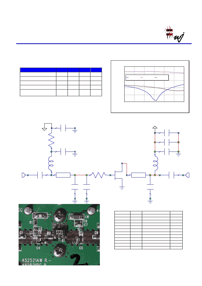
Reference Design: 2400 – 2600 MHz
The application circuit is matched for output power.
Typical RF Performance
Drain Bias = +8 V, I
ds
= 250 mA, 25
°
C
Frequency
MHz
2400
2500
S21 – Gain
dB
12.9
13.0
S11 – Input Return Loss
dB
-14.5
-26
S22 – Output Return Loss
dB
-7.9
-9.6
Output P1dB
dBm
+31.1
+31.2
Output IP3
(+15 dBm / tone, 1 MHz spacing)
2600
12.6
-15
-11.4
+30.8
dBm
+45.0
+45.3
+47.0
The 2.4 – 2.6 GHz Reference Circuit is shown for design purposes only. An
evaluation board is not readily available for this application. The reader can
obtain an FP2189-PCB2140S evaluation board and modify it with the circuit
shown to achieve the performance shown in this reference design.
2.2
2.3
2.4
2.5
2.6
2.7
2.8
Frequency (GHz)
S-Parameters
-30
-20
-10
0
10
20
(
DB(|S[1,1]|)
DB(|S[2,1]|)
DB(|S[2,2]|)
IRES
R=
5.6 Ohm
R2
CAP
C=
DNP pF
C4
IND
ID=
L=
5.6 nH
L1
RES
R=
10 Ohm
R1
CAP
C=
22 pF
C1
CAP
ID=
C=
DNP pF
C2
IIND
L=
18 nH
L2
ICAP
C=
1000 pF
C7
CAP
ID=
C=
22 pF
C6
CAP
ID=
C=
1e4 pF
C8
CAP
C=
22 pF
C9
ICAP
C=
1.3 pF
C5
ICAP
C=
1.8 pF
C11
CAP
ID=
C=
33 pF
C3
TLIN
F0=
EL=
Z0=
2400 MHz
11.8 Deg
50 Ohm
TL1
TLIN
F0=
EL=
Z0=
2400 MHz
23.5 Deg
50 Ohm
TL2
1
2
SID=
NET=
"FP2189"
Q1
PORT
P=
50 Ohm
Z=
1
P2
P=
50 Ohm
Z=
-Vgg
Vds=8V @ 250 mA
14 mil GETEK
TM
ML200DSS (e
r
= 4.2)
The main microstrip line has a line impedance of 50 O.
Bill of Materials
Part style
Chip capacitor
Chip capacitor
Chip capacitor
Chip capacitor
1000 pF
0.1
μ
F
5.6 nH
Multilayer chip inductor
18 nH
Multilayer chip inductor
10 O
Chip resistor
5.6 O
Chip resistor
FP2189
WJ 1W HFET
Do Not Place
Ref. Desig.
C1, C6, C9
C3
C5
C11
C7
C8
L1
L2
R1
R2
Q1
C2, C4
Value
22 pF
33 pF
1.3 pF
1.8 pF
Size
0603
0805
0603
0603
0603
1206
0603
0603
0603
0603
SOT-89
Chip capacitor
Chip capacitor
相關(guān)PDF資料 |
PDF描述 |
|---|---|
| FP218 | TRANSISTOR | BJT | PAIR | PNP | 100V V(BR)CEO | 1A I(C) | FP |
| FP22.2 | TRANSISTOR | JFET | P-CHANNEL | 100UA I(DSS) | CHIP |
| FP25R12KE3V1 | IGBT Module |
| FP25R12KS4CV2 | IGBT Module |
| FP30D250E | Industrial Control IC |
相關(guān)代理商/技術(shù)參數(shù) |
參數(shù)描述 |
|---|---|
| FP2189TR-G | 制造商:TriQuint Semiconductor 功能描述:RF SMALL SIGNAL TRANSISTOR HFET |
| FP21-HST,-3/4\X-48\-BLACK | 制造商:TE Connectivity 功能描述:Heat Shrink Tubing |
| FP21-HST-BLACK-UNMKD-3/4\X | 制造商:TE Connectivity 功能描述:Cable Accessories Jacket Tubing Polyolefin Black Reel |
| FP21THINHST 1/2X48 CLR | 制造商:TE Connectivity 功能描述: |
發(fā)布緊急采購,3分鐘左右您將得到回復(fù)。