- 您現(xiàn)在的位置:買賣IC網(wǎng) > PDF目錄375767 > FDC2612 (FAIRCHILD SEMICONDUCTOR CORP) 200V N-Channel PowerTrench MOSFET PDF資料下載
參數(shù)資料
| 型號: | FDC2612 |
| 廠商: | FAIRCHILD SEMICONDUCTOR CORP |
| 元件分類: | 小信號晶體管 |
| 英文描述: | 200V N-Channel PowerTrench MOSFET |
| 中文描述: | 1100 mA, 200 V, N-CHANNEL, Si, SMALL SIGNAL, MOSFET |
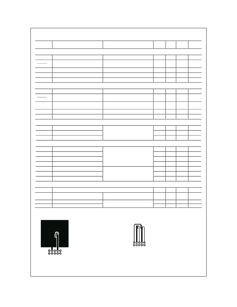
| 封裝: | LEAD FREE, SUPERSOT-6 |
| 文件頁數(shù): | 2/5頁 |
| 文件大小: | 201K |
| 代理商: | FDC2612 |
FDC2612 Rev B3(W)
Electrical Characteristics
T
A
= 25°C unless otherwise noted
Symbol
Parameter
Test Conditions
Min Typ Max Units
Off Characteristics
BV
DSS
Drain–Source Breakdown Voltage
BV
DSS
T
J
Coefficient
I
DSS
Zero Gate Voltage Drain Current
I
GSSF
Gate–Body Leakage, Forward
I
GSSR
Gate–Body Leakage, Reverse
V
GS
= 0 V,
I
D
= 250
μ
A
200
V
Breakdown Voltage Temperature
I
D
= 250
μ
A, Referenced to 25
°
C
246
mV/
°
C
V
DS
= 160 V,
V
GS
= 20 V,
V
GS
= –20 V , V
DS
= 0 V
V
GS
= 0 V
V
DS
= 0 V
1
μ
A
nA
nA
100
–100
On Characteristics
V
GS(th)
Gate Threshold Voltage
V
GS(th)
T
J
Temperature Coefficient
Static Drain–Source
On Resistance
I
D(on)
On–State Drain Current
g
FS
Forward Transconductance
(Note 2)
V
DS
= V
GS
,
I
D
= 250
μ
A, Referenced to 25
°
C
V
GS
= 10 V,
I
D
= 1.1 A
V
GS
= 10 V, I
D
= 1.1 A, T
J
= 125
°
C
V
GS
= 10 V,
V
DS
= 10 V
V
DS
= 10 V,
I
D
= 1.1 A
I
D
= 250
μ
A
2
4
4.5
V
Gate Threshold Voltage
–8.7
mV/
°
C
R
DS(on)
605
1133
4.4
725
1430
m
A
S
4
Dynamic Characteristics
C
iss
Input Capacitance
C
oss
Output Capacitance
C
rss
Reverse Transfer Capacitance
234
18
8
pF
pF
pF
V
DS
= 100 V,
f = 1.0 MHz
V
GS
= 0 V,
Switching Characteristics
(Note 2)
t
d(on)
Turn–On Delay Time
t
r
Turn–On Rise Time
t
d(off)
Turn–Off Delay Time
t
f
Turn–Off Fall Time
Q
g
Total Gate Charge
Q
gs
Gate–Source Charge
Q
gd
Gate–Drain Charge
6
6
17
8
8
1.6
2.2
12
12
30
16
11
ns
ns
ns
ns
nC
nC
nC
V
DD
= 100 V,
V
GS
= 10 V,
I
D
= 1 A,
R
GEN
= 6
V
DS
= 100 V,
V
GS
= 10 V
I
D
= 1.1 A,
Drain–Source Diode Characteristics and Maximum Ratings
I
S
Maximum Continuous Drain–Source Diode Forward Current
Drain–Source Diode Forward
Voltage
t
rr
Diode Reverse Recovery Time
Q
rr
Diode Reverse Recovery Charge
Notes:
1.
R
θ
JA
is the sum of the junction-to-case and case-to-ambient thermal resistance where the case thermal reference is defined as the solder mounting surface of
the drain pins. R
θ
JC
is guaranteed by design while R
θ
CA
is determined by the user's board design.
1.3
A
V
SD
V
GS
= 0 V,
I
S
= 1.3 A
(Note 2)
0.8
1.2
V
74.5
194
nS
nC
I
F
= 1.1A,
d
iF
/d
t
= 300 A/μs
(Note 2)
a)
78°C/W when
mounted on a 1in
2
pad
of 2 oz copper
b)
156°C/W when mounted
on a minimum pad of 2 oz
copper
Scale 1 : 1 on letter size paper
2.
Pulse Test: Pulse Width < 300
μ
s, Duty Cycle < 2.0%
F
相關(guān)PDF資料 |
PDF描述 |
|---|---|
| FDC3512 | 80V N-Channel PowerTrench MOSFET |
| FDC3601N | Dual N-Channel 100V Specified PowerTrench MOSFET |
| FDC3612 | 100V N-Channel PowerTrench MOSFET |
| FDC3616N | 100V N-Channel PowerTrench MOSFET |
| FDC37N958FR | Notebook I/O Controller with Enhanced Keyboard and System Control |
相關(guān)代理商/技術(shù)參數(shù) |
參數(shù)描述 |
|---|---|
| FDC2612_F095 | 功能描述:MOSFET 200V 1.1A N-CH POWERTRENCH RoHS:否 制造商:STMicroelectronics 晶體管極性:N-Channel 汲極/源極擊穿電壓:650 V 閘/源擊穿電壓:25 V 漏極連續(xù)電流:130 A 電阻汲極/源極 RDS(導(dǎo)通):0.014 Ohms 配置:Single 最大工作溫度: 安裝風(fēng)格:Through Hole 封裝 / 箱體:Max247 封裝:Tube |
| FDC2710 | 制造商:M/A-COM Technology Solutions 功能描述:FREQUENCY DOUBLER - Bulk 制造商:M/A-COM Technology Solutions 功能描述:FREQUENCY MULTIPLIER |
| FDC2755C | 制造商:ELMEC 功能描述: |
| FDC2-TB | 制造商:Thomas & Betts 功能描述:3/4", 1G-DEEP BOX, IRON, THRU-FEED 制造商:Thomas & Betts 功能描述:Fittings Gang Box 0.75inch Female Iron |
| FDC2XPTAM39S181A ND | 功能描述:D-Sub標(biāo)準(zhǔn)連接器 15P M FLT SELECT R/A .318 NO SPACER PLATE RoHS:否 制造商:Omron Electronics 位置/觸點數(shù)量:9 排數(shù):2 型式:Female 安裝風(fēng)格:Through Hole 安裝角:Right 端接類型:Solder 過濾: |
發(fā)布緊急采購,3分鐘左右您將得到回復(fù)。