- 您現(xiàn)在的位置:買賣IC網(wǎng) > PDF目錄375725 > FAN53180 (Fairchild Semiconductor Corporation) 6-Bit VID Controlled 2-4 Phase DC-DC Controller PDF資料下載
參數(shù)資料
| 型號: | FAN53180 |
| 廠商: | Fairchild Semiconductor Corporation |
| 英文描述: | 6-Bit VID Controlled 2-4 Phase DC-DC Controller |
| 中文描述: | 6位VID控制2-4相DC - DC控制器 |
| 文件頁數(shù): | 22/28頁 |
| 文件大?。?/td> | 851K |
| 代理商: | FAN53180 |
第1頁第2頁第3頁第4頁第5頁第6頁第7頁第8頁第9頁第10頁第11頁第12頁第13頁第14頁第15頁第16頁第17頁第18頁第19頁第20頁第21頁當前第22頁第23頁第24頁第25頁第26頁第27頁第28頁
FAN53180
PRODUCT SPECIFICATION
22
REV. 1.0.0 6/10/03
With the multimode feedback structure of the FAN53180,
one needs to set the feedback compensation to make the
converter’s output impedance working in parallel with the
output decoupling meet this goal. There are several poles and
zeros created by the output inductor and decoupling capaci-
tors (output filter) that need to be compensated for.
A type-three compensator on the voltage feedback is
adequate for proper compensation of the output filter. The
expressions given in Equations 25–29 are intended to yield
an optimal starting point for the design; some adjustments
may be necessary to account for PCB and component para-
sitic effects (see the Tuning Procedure for the FAN53180
section).
The first step is to compute the time constants for all of the
poles and zeros in the system:
where, for the FAN53180, R’ is the PCB resistance from the
bulk capacitors to the ceramics and where R
DS
is approxi-
mately the total low-side MOSFET ON resistance per phase
at 25oC. For this example, A
D
is 5, V
RT
equals 0.974V, R’ is
approximately 0.6m
(assuming a 4-layer motherboard) and
L
X
is 375pH for the eight Al-Poly capacitors.
The compensation values can then be solved for using the
following:
Choosing the closest standard values for these components
yields: C
A
= 390pF, R
A
= 16.9k
, C
B
= 1.5nF, and
C
FB
= 33pF.
C
IN
Selection and Input Current di/dt Reduction
In continuous inductor-current mode, the source current of
the high-side MOSFET is approximately a square wave with
a duty ratio equal to n (V
OUT
/V
IN
) and an amplitude of one-
nth of the maximum output current. To prevent large voltage
transients, a low ESR input capacitor sized for the maximum
rms current must be used. The maximum rms capacitor cur-
rent is given by:
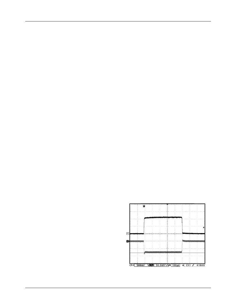
Figure 6. Typical Transient Response for Design Example
R
E
n
R
O
A
D
R
DS
+
R
----------------------
V
×
VID
2
--------------------------------------------------------
L
×
1 n
–
(
X
D
×
)
V
RT
×
×
O
VID
+
+
×
×
=
(25)
R
E
3
1.3m
5
5.95m
-------------------------------------------
+
+
×
+
×
=
----------------------------------------–
)
0.974V
1.5V
×
×
55.3m
=
T
A
C
X
R
O
R
'
–
(
)
L
X
R
O
-------
R
-------------------
R
'
–
X
×
+
×
=
(26)
T
A
6.56mF
1.3m
0.6m
–
(
)
------------------
×
+
×
=
--------------------–
4.79
μ
s
=
T
B
R
X
R
'
R
O
–
+
(
)
C
X
×
=
(27)
T
B
1.0m
0.6m
1.3m
–
+
(
)
6.56mF
×
1.97
μ
s
=
=
T
C
V
RT
--------------------------------------------------------
L
A
R
×
------------------------
–
×
VID
E
=
(28)
T
C
0.974V
--------------------------------------------------------------------------------------
650nH
-------------------------------
–
×
6.86
μ
s
=
=
T
D
C
O
C
'
–
C
Z
+
C
X
R
O
------------------------------------------------------------------
=
(29)
T
D
1.3m
220
μ
F
+
(
)
2
×
)
1.3m
×
--------------------------------------------------–
500ns
=
=
C
A
n
------------------------------
R
×
E
T
A
×
B
=
(30)
C
A
----------------------------------------------------
s
253pF
=
=
R
A
T
C
C
A
-------
s
------------------
27.1k
=
=
=
(31)
C
B
T
B
R
B
-------
s
-------------------
1.48nF
=
=
=
(32)
C
FB
T
D
R
A
-------
-------------------
18.5pF
=
=
=
(33)
相關PDF資料 |
PDF描述 |
|---|---|
| FAN5330 | High Efficiency Serial LED Driver with 30V Integrated Switch |
| FAN5331 | 1.6MHz Boost Converter with 20V Integrated FET Switch |
| FAN5331SX | 1.6MHz Boost Converter with 20V Integrated FET Switch |
| FAN5332A | High Efficiency, High Current Serial LED Driver and OLED Supply with 30V Integrated Switch |
| FAN5332ASX | High Efficiency, High Current Serial LED Driver and OLED Supply with 30V Integrated Switch |
相關代理商/技術參數(shù) |
參數(shù)描述 |
|---|---|
| FAN53180MTC | 制造商:FAIRCHILD 制造商全稱:Fairchild Semiconductor 功能描述:6-Bit VID Controlled 2-4 Phase DC-DC Controller |
| FAN53180MTCX | 功能描述:DC/DC 開關控制器 Buck Controller 2to4 Phs VID Sync RoHS:否 制造商:Texas Instruments 輸入電壓:6 V to 100 V 開關頻率: 輸出電壓:1.215 V to 80 V 輸出電流:3.5 A 輸出端數(shù)量:1 最大工作溫度:+ 125 C 安裝風格: 封裝 / 箱體:CPAK |
| FAN5330 | 制造商:FAIRCHILD 制造商全稱:Fairchild Semiconductor 功能描述:High Efficiency Serial LED Driver with 30V Integrated Switch |
| FAN5330SX | 功能描述:LED照明驅動器 SYSTEM_POWER RoHS:否 制造商:STMicroelectronics 輸入電壓:11.5 V to 23 V 工作頻率: 最大電源電流:1.7 mA 輸出電流: 最大工作溫度: 安裝風格:SMD/SMT 封裝 / 箱體:SO-16N |
| FAN5331 | 制造商:FAIRCHILD 制造商全稱:Fairchild Semiconductor 功能描述:High Efficiency Serial LED Driver and OLED Supply with 20V Integrated Switch |
發(fā)布緊急采購,3分鐘左右您將得到回復。