- 您現(xiàn)在的位置:買賣IC網(wǎng) > PDF目錄375725 > FAN53180 (Fairchild Semiconductor Corporation) 6-Bit VID Controlled 2-4 Phase DC-DC Controller PDF資料下載
參數(shù)資料
| 型號: | FAN53180 |
| 廠商: | Fairchild Semiconductor Corporation |
| 英文描述: | 6-Bit VID Controlled 2-4 Phase DC-DC Controller |
| 中文描述: | 6位VID控制2-4相DC - DC控制器 |
| 文件頁數(shù): | 15/28頁 |
| 文件大小: | 851K |
| 代理商: | FAN53180 |
第1頁第2頁第3頁第4頁第5頁第6頁第7頁第8頁第9頁第10頁第11頁第12頁第13頁第14頁當(dāng)前第15頁第16頁第17頁第18頁第19頁第20頁第21頁第22頁第23頁第24頁第25頁第26頁第27頁第28頁

PRODUCT SPECIFICATION
FAN53180
REV. 1.0.0 6/10/03
15
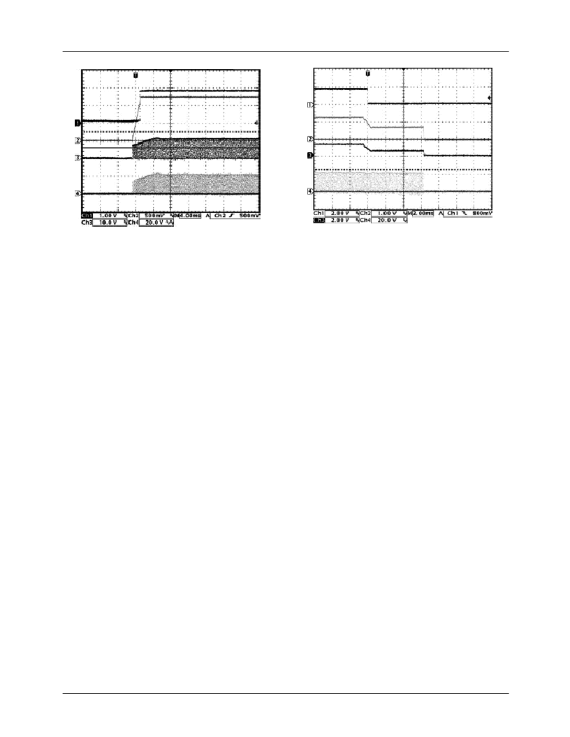
Figure 2. Start-Up Waveforms, Circuit of Figure 1
Channel 1 – PWRGD
Channel 2 – V
OUT
Channel 3 – HS MOSFET V
GS
Channel 4 – LS MOSFET V
GS
After the limit is reached, the 3V pull-up on the DELAY
pin is disconnected, and the external delay capacitor is dis-
charged through the external resistor. A comparator monitors
the DELAY voltage and shuts off the controller when the
voltage drops below 1.8V. The current limit latch off delay
time is therefore set by the RC time constant discharging
from 3V to 1.8V. The applications section discusses the
selection of C
DLY
and R
DLY
.
Because the controller continues to cycle the phases during
the latch-off delay time, if the short is removed before the
1.8V threshold is reached, the controller will return to
normal operation. The recovery characteristic depends on the
state of PWRGD. If the output voltage is within the PWRGD
window, the controller resumes normal operation. However,
if short circuit has caused the output voltage to drop below
the PWRGD threshold, then a soft-start cycle is initiated.
The latch-off function can be reset by either removing and re-
applying VCC to the FAN53180, or by pulling the EN pin low
for a short time. To disable the short circuit latchoff function,
the external resistor to ground should be left open, and a large
(greater than 1M
) resistor should be connected from VCC to
DELAY. This prevents the DELAY capacitor from discharging
so the 1.8V threshold is never reached. The resistor will have an
impact on the soft-start time because the current through it will
add to the internal 20μA current source.
During start-up when the output voltage is below 200mV,
a secondary current limit is active. This is necessary because
the voltage swing of CSCOMP cannot go below ground.
This secondary current limit controls the internal COMP
voltage to the PWM comparators to 2V. This will limit the
voltage drop across the low side MOSFETs through the
current balance circuitry.
Figure 3. Overcurrent Latch Off Waveform,
Circuit of Figure 1
Channel 1 – PWRGD
Channel 2 – V
OUT
Channel 3 – CSCOMP
Channel 4 – HS MOSFET V
GS
There is also an inherent per phase current limit that will
protect individual phases in the case where one or more
phases may stop functioning because of a faulty component.
This limit is based on the maximum normal-mode COMP
voltage.
Dynamic VID
The FAN53180 incorporates the ability to dynamically
change the VID input while the controller is running.
This allows the output voltage to change while the supply
is running and supplying current to the load. This is com-
monly referred to as VID-on-the-fly (OTF). A VID-OTF
can occur under either light load or heavy load conditions.
The processor signals the controller by changing the VID
inputs in multiple steps from the start code to the finish code.
This change can be either positive or negative.
When a VID input changes state, the FAN53180 detects the
change and ignores the DAC inputs for a minimum of 400ns.
This time is to prevent a false code due to logic skew while
the six VID inputs are changing. Additionally, the first VID
change initiates the PWRGD and CROWBAR blanking
functions for a minimum of 250μs to prevent a false
PWRGD or CROWBAR event. Each VID change will reset
the internal timer.
Figure 4 shows VID on-the-fly perfor-
mance when the output voltage is stepping up and the output
current is switching between minimum and maximum
values, which is the worst-case situation.
相關(guān)PDF資料 |
PDF描述 |
|---|---|
| FAN5330 | High Efficiency Serial LED Driver with 30V Integrated Switch |
| FAN5331 | 1.6MHz Boost Converter with 20V Integrated FET Switch |
| FAN5331SX | 1.6MHz Boost Converter with 20V Integrated FET Switch |
| FAN5332A | High Efficiency, High Current Serial LED Driver and OLED Supply with 30V Integrated Switch |
| FAN5332ASX | High Efficiency, High Current Serial LED Driver and OLED Supply with 30V Integrated Switch |
相關(guān)代理商/技術(shù)參數(shù) |
參數(shù)描述 |
|---|---|
| FAN53180MTC | 制造商:FAIRCHILD 制造商全稱:Fairchild Semiconductor 功能描述:6-Bit VID Controlled 2-4 Phase DC-DC Controller |
| FAN53180MTCX | 功能描述:DC/DC 開關(guān)控制器 Buck Controller 2to4 Phs VID Sync RoHS:否 制造商:Texas Instruments 輸入電壓:6 V to 100 V 開關(guān)頻率: 輸出電壓:1.215 V to 80 V 輸出電流:3.5 A 輸出端數(shù)量:1 最大工作溫度:+ 125 C 安裝風(fēng)格: 封裝 / 箱體:CPAK |
| FAN5330 | 制造商:FAIRCHILD 制造商全稱:Fairchild Semiconductor 功能描述:High Efficiency Serial LED Driver with 30V Integrated Switch |
| FAN5330SX | 功能描述:LED照明驅(qū)動器 SYSTEM_POWER RoHS:否 制造商:STMicroelectronics 輸入電壓:11.5 V to 23 V 工作頻率: 最大電源電流:1.7 mA 輸出電流: 最大工作溫度: 安裝風(fēng)格:SMD/SMT 封裝 / 箱體:SO-16N |
| FAN5331 | 制造商:FAIRCHILD 制造商全稱:Fairchild Semiconductor 功能描述:High Efficiency Serial LED Driver and OLED Supply with 20V Integrated Switch |
發(fā)布緊急采購,3分鐘左右您將得到回復(fù)。