- 您現(xiàn)在的位置:買賣IC網(wǎng) > PDF目錄17052 > EVAL-AD7329CBZ (Analog Devices Inc)BOARD EVALUATION FOR AD7329CBZ PDF資料下載
參數(shù)資料
| 型號(hào): | EVAL-AD7329CBZ |
| 廠商: | Analog Devices Inc |
| 文件頁數(shù): | 40/41頁 |
| 文件大小: | 0K |
| 描述: | BOARD EVALUATION FOR AD7329CBZ |
| 標(biāo)準(zhǔn)包裝: | 1 |
| 系列: | iCMOS® |
| ADC 的數(shù)量: | 1 |
| 位數(shù): | 12 |
| 采樣率(每秒): | 1M |
| 數(shù)據(jù)接口: | 串行 |
| 輸入范圍: | ±10 V |
| 在以下條件下的電源(標(biāo)準(zhǔn)): | 30mW @ 1MSPS |
| 工作溫度: | -40°C ~ 85°C |
| 已用 IC / 零件: | AD7329 |
| 已供物品: | 板 |
| 相關(guān)產(chǎn)品: | AD7329BRUZ-REEL7-ND - IC ADC 12BIT+SAR 8CHAN 24-TSSOP AD7329BRUZ-REEL-ND - IC ADC 12BIT+SAR 8CHAN 24-TSSOP AD7329BRUZ-ND - IC ADC 12BIT 8CH MUX SPI 24TSSOP |
第1頁第2頁第3頁第4頁第5頁第6頁第7頁第8頁第9頁第10頁第11頁第12頁第13頁第14頁第15頁第16頁第17頁第18頁第19頁第20頁第21頁第22頁第23頁第24頁第25頁第26頁第27頁第28頁第29頁第30頁第31頁第32頁第33頁第34頁第35頁第36頁第37頁第38頁第39頁當(dāng)前第40頁第41頁
Data Sheet
AD7329
Rev. B | Page 7 of 40
TIMING SPECIFICATIONS
VDD = 12 V to 16.5 V, VSS = 12 V to 16.5 V, VCC = 4.75 V to 5.25 V, VDRIVE = 2.7 V to 5.25 V, VREF = 2.5 V internal/external, TA = TMAX to
TMIN. Timing specifications apply with a 32 pF load, unless otherwise noted. MUXOUT+ is connected directly to ADCIN+ and MUXOUT is
connected directly to ADCIN, which is connected to GND for single-ended mode.
Table 3.
Limit at TMIN, TMAX
Description
Parameter
VCC < 4.75 V
VCC = 4.75 V to 5.25 V
Unit
VDRIVE ≤ VCC
fSCLK
50
kHz min
14
20
MHz max
tCONVERT
16 × tSCLK
ns max
tSCLK = 1/fSCLK
tQUIET
75
60
ns min
Minimum time between end of serial read and next falling edge of CS
t1
12
5
ns min
Minimum CS pulse width
t21
25
20
ns min
CS to SCLK setup time; bipolar input ranges (±10 V, ±5 V, ±2.5 V)
45
35
ns min
Unipolar input range (0 V to 10 V)
t3
26
14
ns max
Delay from CS until DOUT three-state disabled
t4
57
43
ns max
Data access time after SCLK falling edge
t5
0.4 × tSCLK
ns min
SCLK low pulse width
t6
0.4 × tSCLK
ns min
SCLK high pulse width
t7
13
8
ns min
SCLK to data valid hold time
t8
40
22
ns max
SCLK falling edge to DOUT high impedance
10
9
ns min
SCLK falling edge to DOUT high impedance
t9
4
ns min
DIN setup time prior to SCLK falling edge
t10
2
ns min
DIN hold time after SCLK falling edge
tPOWER-UP
750
ns max
Power-up from autostandby
500
s max
Power-up from full shutdown/autoshutdown mode, internal
reference
25
s typ
Power-up from full shutdown/autoshutdown mode, external
reference
1
When using VCC = 4.75 V to 5.25 V and the 0 V to 10 V unipolar range, running at 1 MSPS throughput rate with t2 at 20 ns, the mark-space ratio must be limited to 50:50.
ADD1
1
2
3
4
5
13
14
15
16
WRITE
REG
SEL1
REG
SEL2
LSB
0
MSB
ADD0
SIGN
DB11
DB10
DB2
DB1
DB0
t2
t6
t4
t9
t10
t3
t7
t5
t8
t1
tQUIET
tCONVERT
SCLK
CS
DOUT
THREE-
STATE
THREE-STATE
DIN
ADD2
3 IDENTIFICATION BITS
05402-
002
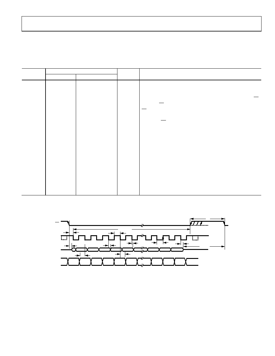
Figure 2. Serial Interface Timing Diagram
相關(guān)PDF資料 |
PDF描述 |
|---|---|
| ACC05DRTS | CONN EDGECARD 10POS .100 DIP SLD |
| LQW2BAS10NJ00L | INDUCTOR RF 10NH 600MA 0805 |
| ACC07DREF | CONN EDGECARD 14POS .100 EYELET |
| 0210391054 | CABLE JUMPER 1MM .051M 35POS |
| EVAL-AD7324CBZ | BOARD EVALUATION FOR AD7324CBZ |
相關(guān)代理商/技術(shù)參數(shù) |
參數(shù)描述 |
|---|---|
| EVAL-AD73311EB | 制造商:AD 制造商全稱:Analog Devices 功能描述:Low Cost, Low Power CMOS General Purpose Analog Front End |
| EVAL-AD73311EZ | 制造商:AD 制造商全稱:Analog Devices 功能描述:Low Cost, Low Power CMOS General Purpose Analog Front End |
| EVAL-AD73311LEB | 制造商:AD 制造商全稱:Analog Devices 功能描述:Low Cost, Low Power CMOS General Purpose Analog Front End |
| EVAL-AD73322EB | 制造商:AD 制造商全稱:Analog Devices 功能描述:Low Cost, Low Power CMOS General-Purpose Dual Analog Front End |
| EVAL-AD73322EZ | 制造商:AD 制造商全稱:Analog Devices 功能描述:Low Cost, Low Power CMOS General-Purpose Dual Analog Front End |
發(fā)布緊急采購,3分鐘左右您將得到回復(fù)。