- 您現(xiàn)在的位置:買賣IC網(wǎng) > PDF目錄97913 > EP1K50FI484-2DX Field Programmable Gate Array (FPGA) PDF資料下載
參數(shù)資料
| 型號: | EP1K50FI484-2DX |
| 英文描述: | Field Programmable Gate Array (FPGA) |
| 中文描述: | 現(xiàn)場可編程門陣列(FPGA) |
| 文件頁數(shù): | 32/86頁 |
| 文件大?。?/td> | 1263K |
| 代理商: | EP1K50FI484-2DX |
第1頁第2頁第3頁第4頁第5頁第6頁第7頁第8頁第9頁第10頁第11頁第12頁第13頁第14頁第15頁第16頁第17頁第18頁第19頁第20頁第21頁第22頁第23頁第24頁第25頁第26頁第27頁第28頁第29頁第30頁第31頁當(dāng)前第32頁第33頁第34頁第35頁第36頁第37頁第38頁第39頁第40頁第41頁第42頁第43頁第44頁第45頁第46頁第47頁第48頁第49頁第50頁第51頁第52頁第53頁第54頁第55頁第56頁第57頁第58頁第59頁第60頁第61頁第62頁第63頁第64頁第65頁第66頁第67頁第68頁第69頁第70頁第71頁第72頁第73頁第74頁第75頁第76頁第77頁第78頁第79頁第80頁第81頁第82頁第83頁第84頁第85頁第86頁
38
Altera Corporation
ACEX 1K Programmable Logic Device Family Data Sheet
for -1 and -2 speed-grade devices, respectively.
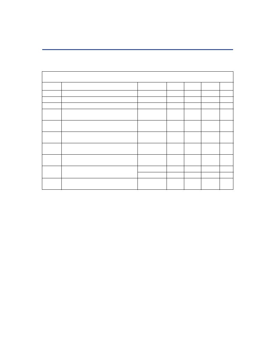
Table 11. ClockLock & ClockBoost Parameters for -1 Speed-Grade Devices
Symbol
Parameter
Condition
Min
Typ
Max
Unit
tR
Input rise time
5
ns
tF
Input fall time
5ns
tINDUTY
Input duty cycle
40
60
%
fCLK1
Input clock frequency (ClockBoost clock
multiplication factor equals 1)
25
180
MHz
fCLK2
Input clock frequency (ClockBoost clock
multiplication factor equals 2)
16
90
MHz
fCLKDEV
Input deviation from user specification in the
Altera software (1)
25,000
PPM
tINCLKSTB Input clock stability (measured between
adjacent clocks)
100
ps
tLOCK
Time required for ClockLock or ClockBoost
to acquire lock (3)
10
s
tJITTER
Jitter on ClockLock or ClockBoost-
generated clock (4)
tINCLKSTB <100
250 (4)
ps
tINCLKSTB < 50
200 (4)
ps
tOUTDUTY Duty cycle for ClockLock or ClockBoost-
generated clock
40
50
60
%
相關(guān)PDF資料 |
PDF描述 |
|---|---|
| EP1K50FI484-2F | Field Programmable Gate Array (FPGA) |
| EP1K50FI484-2P | Field Programmable Gate Array (FPGA) |
| EP1K50FI484-2X | Field Programmable Gate Array (FPGA) |
| EP1K50FI484-3F | Field Programmable Gate Array (FPGA) |
| EP1K50QC208-1DX | Field Programmable Gate Array (FPGA) |
相關(guān)代理商/技術(shù)參數(shù) |
參數(shù)描述 |
|---|---|
| EP1K50FI484-2F | 制造商:未知廠家 制造商全稱:未知廠家 功能描述:Field Programmable Gate Array (FPGA) |
| EP1K50FI484-2P | 制造商:未知廠家 制造商全稱:未知廠家 功能描述:Field Programmable Gate Array (FPGA) |
| EP1K50FI484-2X | 制造商:未知廠家 制造商全稱:未知廠家 功能描述:Field Programmable Gate Array (FPGA) |
| EP1K50FI484-3F | 制造商:未知廠家 制造商全稱:未知廠家 功能描述:Field Programmable Gate Array (FPGA) |
| EP1K50QC2081 | 制造商:ALTERA 功能描述:* |
發(fā)布緊急采購,3分鐘左右您將得到回復(fù)。