- 您現(xiàn)在的位置:買賣IC網(wǎng) > PDF目錄384277 > EDD1216AJTA-6B-E (ELPIDA MEMORY INC) 128M bits DDR SDRAM PDF資料下載
參數(shù)資料
| 型號: | EDD1216AJTA-6B-E |
| 廠商: | ELPIDA MEMORY INC |
| 元件分類: | DRAM |
| 英文描述: | 128M bits DDR SDRAM |
| 中文描述: | 8M X 16 DDR DRAM, 0.7 ns, PDSO66 |
| 封裝: | ROHS COMPLIANT, PLASTIC, TSOP2-66 |
| 文件頁數(shù): | 16/52頁 |
| 文件大小: | 513K |
| 代理商: | EDD1216AJTA-6B-E |
第1頁第2頁第3頁第4頁第5頁第6頁第7頁第8頁第9頁第10頁第11頁第12頁第13頁第14頁第15頁當前第16頁第17頁第18頁第19頁第20頁第21頁第22頁第23頁第24頁第25頁第26頁第27頁第28頁第29頁第30頁第31頁第32頁第33頁第34頁第35頁第36頁第37頁第38頁第39頁第40頁第41頁第42頁第43頁第44頁第45頁第46頁第47頁第48頁第49頁第50頁第51頁第52頁
EDD1216AJTA
Data Sheet E0972E30 (Ver. 3.0)
16
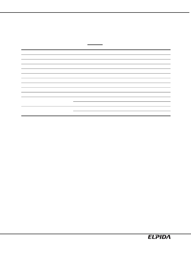
Command Operation
Command Truth Table
DDR SDRAM recognize the following commands specified by the /CS, /RAS, /CAS, /WE and address pins. All other
combinations than those in the table below are illegal.
CKE
Command
Symbol
n – 1 n
/CS
/RAS /CAS /WE BA1 BA0 AP
Address
Ignore command
DESL
H
H
H
×
×
×
×
×
×
×
No operation
NOP
H
H
L
H
H
H
×
×
×
×
Burst stop in read command
BST
H
H
L
H
H
L
×
×
×
×
Column address and read command
READ
H
H
L
H
L
H
V
V
L
V
Read with auto-precharge
READA
H
H
L
H
L
H
V
V
H
V
Column address and write command
WRIT
H
H
L
H
L
L
V
V
L
V
Write with auto-precharge
WRITA
H
H
L
H
L
L
V
V
H
V
Row address strobe and bank active
ACT
H
H
L
L
H
H
V
V
V
V
Precharge select bank
PRE
H
H
L
L
H
L
V
V
L
×
Precharge all bank
PALL
H
H
L
L
H
L
×
×
H
×
Refresh
REF
H
H
L
L
L
H
×
×
×
×
SELF
H
L
L
L
L
H
×
×
×
×
Mode register set
MRS
H
H
L
L
L
L
L
L
L
V
Remark: H: VIH. L: VIL.
×
: VIH or VIL V: Valid address input
Note: The CKE level must be kept for 1 CK cycle at least.
Ignore command [DESL]
When /CS is high at the cross point of the CK rising edge and the VREF level, every input are neglected and internal
status is held.
No operation [NOP]
As long as this command is input at the cross point of the CK rising edge and the VREF level, address and data
input are neglected and internal status is held.
Burst stop in read operation [BST]
This command stops a burst read operation, which is not applicable for a burst write operation.
Column address strobe and read command [READ]
This command starts a read operation. The start address of the burst read is determined by the column address
(See “Address Pins Table” in Pin Function) and the bank select address. After the completion of the read operation,
the output buffer becomes high-Z.
Read with auto-precharge [READA]
This command starts a read operation. After completion of the read operation, precharge is automatically executed.
Column address strobe and write command [WRIT]
This command starts a write operation. The start address of the burst write is determined by the column address
(See “Address Pins Table” in Pin Function) and the bank select address.
Write with auto-precharge [WRITA]
This command starts a write operation. After completion of the write operation, precharge is automatically executed.
EMRS
H
H
L
L
L
L
L
H
L
V
相關PDF資料 |
PDF描述 |
|---|---|
| EDD1216AJTA-7A-E | 128M bits DDR SDRAM |
| EDD1216AJTA-7B-E | 128M bits DDR SDRAM |
| EDD1232AABH | 128M bits DDR SDRAM (4M words x 32 bits) |
| EDD1232AABH-6B-E | GT 2C 2#0 SKT PLUG |
| EDD1232AAFA | 128M bits DDR SDRAM (4M words x 32 bits) |
相關代理商/技術參數(shù) |
參數(shù)描述 |
|---|---|
| EDD1216AJTA-7A-E | 制造商:ELPIDA 制造商全稱:Elpida Memory 功能描述:128M bits DDR SDRAM |
| EDD1216AJTA-7B-E | 制造商:ELPIDA 制造商全稱:Elpida Memory 功能描述:128M bits DDR SDRAM |
| EDD1216ALTA | 制造商:ELPIDA 制造商全稱:Elpida Memory 功能描述:128 M-bit Synchronous DRAM with Double Data Rate (4-bank, SSTL_2) |
| EDD1216ALTA-1A | 制造商:ELPIDA 制造商全稱:Elpida Memory 功能描述:128 M-bit Synchronous DRAM with Double Data Rate (4-bank, SSTL_2) |
| EDD1216ALTA-75 | 制造商:ELPIDA 制造商全稱:Elpida Memory 功能描述:128 M-bit Synchronous DRAM with Double Data Rate (4-bank, SSTL_2) |
發(fā)布緊急采購,3分鐘左右您將得到回復。