- 您現(xiàn)在的位置:買賣IC網(wǎng) > PDF目錄358702 > DS89C450 Ultra-High-Speed Flash Microcontrollers PDF資料下載
參數(shù)資料
| 型號(hào): | DS89C450 |
| 英文描述: | Ultra-High-Speed Flash Microcontrollers |
| 中文描述: | 超高速閃存微控制器 |
| 文件頁數(shù): | 2/48頁 |
| 文件大?。?/td> | 934K |
| 代理商: | DS89C450 |
第1頁當(dāng)前第2頁第3頁第4頁第5頁第6頁第7頁第8頁第9頁第10頁第11頁第12頁第13頁第14頁第15頁第16頁第17頁第18頁第19頁第20頁第21頁第22頁第23頁第24頁第25頁第26頁第27頁第28頁第29頁第30頁第31頁第32頁第33頁第34頁第35頁第36頁第37頁第38頁第39頁第40頁第41頁第42頁第43頁第44頁第45頁第46頁第47頁第48頁
DS89C430/DS89C44/DS89C450 Ultra-High-Speed Flash Microcontrollers
2 of 48
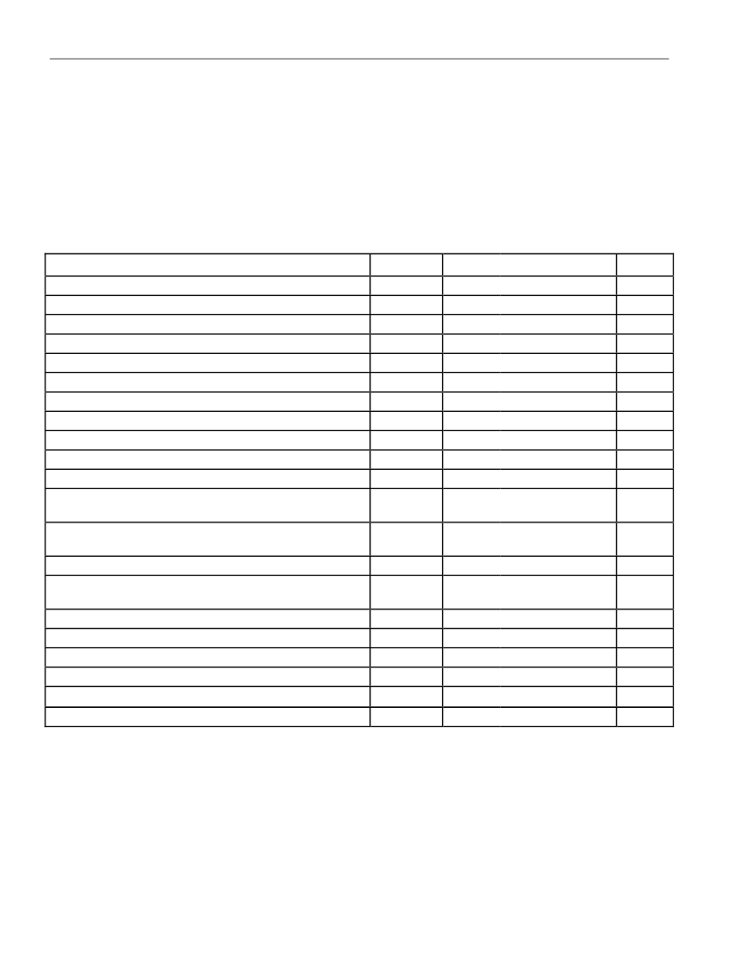
ABSOLUTE MAXIMUM RATINGS
Voltage Range on Any Pin Relative to Ground
Voltage Range on V
CC
Relative to Ground
Ambient Temperature Range (under bias)
Storage Temperature Range
Soldering Temperature
Stresses beyond those listed under “Absolute Maximum Ratings” may cause permanent damage to the device. These are stress ratings only,
and functional operation of the device at these or any other conditions beyond those indicated in the operational sections of the specifications is
not implied. Exposure to the absolute maximum rating conditions for extended periods may affect device reliability.
DC ELECTRICAL CHARACTERISTICS
(V
CC
= 4.5V to 5.5V, T
O
= -40°C to +85°C.) (Note 1)
-0.3V to (V
CC
+ 0.5V)
-0.3V to +6.0V
-40°C to +85°C
-55°C to +125°C
See IPC/JEDEC J-STD-020A
PARAMETER
SYMBOL
MIN
TYP
MAX
UNITS
Supply Voltage (Notes 2, 3)
V
CC
4.5
5.0
5.5
V
Power-Fail Warning (Notes 2, 4)
V
PFW
4.2
4.375
4.6
V
Reset Trip Point (Min Operating Voltage) (Notes 2, 3, 4)
V
RST
3.95
4.125
4.35
V
Supply Current, Active Mode (Note 5)
I
CC
75
110
A
Supply Current, Idle Mode at 33MHz (Note 6)
I
IDLE
40
50
A
Supply Current, Stop Mode, Bandgap Disabled (Note 7)
I
STOP
1
100
A
Supply Current, Stop Mode, Bandgap Enabled (Note 7)
I
SPBG
150
300
A
Input Low Level (Note 2)
V
IL
-0.3
+0.8
V
Input High Level (Note 2)
V
IH
2.0
V
CC
+ 0.3
V
Input High Level XTAL and RST (Note 2)
V
IH2
3.5
V
CC
+ 0.3
V
Output Low Voltage, Port 1 and 3 at I
OL
= 1.6mA (Note 2)
V
OL1
0.15
0.45
V
Output Low Voltage, Port 0 and 2, ALE,
PSEN
at I
OL
= 3.2mA
(Note 2)
V
OL2
0.15
0.45
V
Output High Voltage, Port 1, 2, and 3, at I
OH
= -50 A
(Notes 2, 8)
V
OH1
2.4
V
Output High Voltage, Port 1, 2, and 3 at I
OH
= -1.5mA (Notes 2, 9)
V
OH2
2.4
V
Output High Voltage, Port 0, 1, 2, ALE,
PSEN
,
RD
,
WR
in Bus
Mode at I
OH
= -8mA (Notes 2, 10)
V
OH3
2.4
V
Output High Voltage, RST at I
OL
= -0.4mA (Note 2, 11)
V
OH4
2.4
V
Input Low Current, Port 1, 2, and 3 at 0.4V
I
IL
-50
A
Transition Current from 1 to 0, Port 1, 2, and 3 at 2V (Note 12)
I
TL
-650
A
Input Leakage Current, Port 0 in I/O Mode and
EA
(Note 13)
I
L
-10
+10
A
Input Current, Port 0 in Bus Mode (Note 14)
I
L
-300
+300
A
RST Pulldown Resistance (Note 13)
R
RST
50
120
200
k
相關(guān)PDF資料 |
PDF描述 |
|---|---|
| DS89C21TMX | Transceiver |
| DSDK101 | Low-Cost Demo Kit Motherboard |
| E.FL-LP-040 | CABLE ; Connector type A:MFD-Titan; Connector type B:MFD-Titan; Length, lead:5m |
| E15R8-FREQ-OUT14 | CRYSTAL OSCILLATOR, CLOCK, 30 MHz - 200 MHz, ECL OUTPUT |
| E1L51-AW0A4-05 | T-1 3/4 SINGLE COLOR LED, WHITE, 5 mm |
相關(guān)代理商/技術(shù)參數(shù) |
參數(shù)描述 |
|---|---|
| DS89C450+ENG | 制造商:Maxim Integrated Products 功能描述:MCU 8BIT CISC 64KB FLASH 5V 44TQFP - Trays |
| DS89C450+ENL | 制造商:Maxim Integrated Products 功能描述:MCU 8BIT CISC 64KB FLASH 5V 44TQFP - Trays |
| DS89C450+MNG | 制造商:Maxim Integrated Products 功能描述:MCU 8BIT CISC 64KB FLASH 5V 40PDIP - Rail/Tube |
| DS89C450+MNL | 制造商:Maxim Integrated Products 功能描述:MCU 8BIT CISC 64KB FLASH 5V 40PDIP - Rail/Tube |
| DS89C450+QNL | 制造商:Maxim Integrated Products 功能描述:MICRO HI SPD 44PLCC 64K IND PB-FREE - Rail/Tube |
發(fā)布緊急采購,3分鐘左右您將得到回復(fù)。