- 您現(xiàn)在的位置:買賣IC網(wǎng) > PDF目錄358702 > DS89C430 Ultra-High-Speed Flash Microcontrollers PDF資料下載
參數(shù)資料
| 型號: | DS89C430 |
| 英文描述: | Ultra-High-Speed Flash Microcontrollers |
| 中文描述: | 超高速閃存微控制器 |
| 文件頁數(shù): | 19/48頁 |
| 文件大?。?/td> | 934K |
| 代理商: | DS89C430 |
第1頁第2頁第3頁第4頁第5頁第6頁第7頁第8頁第9頁第10頁第11頁第12頁第13頁第14頁第15頁第16頁第17頁第18頁當(dāng)前第19頁第20頁第21頁第22頁第23頁第24頁第25頁第26頁第27頁第28頁第29頁第30頁第31頁第32頁第33頁第34頁第35頁第36頁第37頁第38頁第39頁第40頁第41頁第42頁第43頁第44頁第45頁第46頁第47頁第48頁
DS89C430/DS89C440/DS89C450 Ultra-High-Speed Flash Microcontrollers
19 of 48
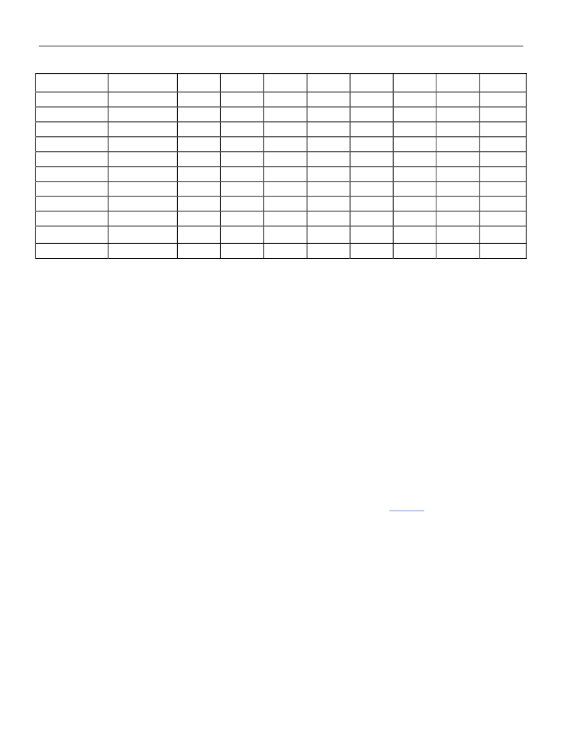
Table 2. SFR Reset Value (continued)
REGISTER
ADDRESS
BIT 7
BIT 6
BIT 5
BIT 4
BIT 3
BIT 2
BIT 1
BIT 0
TL2
CCh
0
0
0
0
0
0
0
0
TH2
CDh
0
0
0
0
0
0
0
0
PSW
D0h
0
0
0
0
0
0
0
0
FCNTL
D5h
1
0
1
1
0
0
0
0
FDATA
D6h
0
0
0
0
0
0
0
0
WDCON
D8h
0
Special
0
Special
0
Special
Special
0
ACC
E0h
0
0
0
0
0
0
0
0
EIE
E8h
1
1
1
0
0
0
0
0
B
F0h
0
0
0
0
0
0
0
0
EIP1
F1h
1
1
1
0
0
0
0
0
EIP0
F8h
1
1
1
0
0
0
0
0
Note:
Consult the
Ultra-High-Speed Flash Microcontroller User’s Guide
for more information about the bits marked “Special.”
Memory Organization
There are three distinct memory areas in the DS89C430: scratchpad registers, program memory, and data
memory. The registers are located on-chip but the program and data memory spaces can be on-chip, off-chip, or
both. The DS89C430/DS89C440/DS89C450 have 16kB/32kB/64kB of on-chip program memory, respectively,
implemented in flash memory and also have 1kB of on-chip data memory space that can be configured as program
space using the PRAME bit in the ROMSIZE feature. The DS89C430 uses a memory-addressing scheme that
separates program memory from data memory. The program and data segments can be overlapped since they are
accessed in different manners. If the maximum address of on-chip program or data memory is exceeded, the
DS89C430 performs an external memory access using the expanded memory bus. The
PSEN
signal goes active
low to serve as a chip enable or output enable when performing a code fetch from external program memory.
MOVX instructions activate the
RD
or
WR
signal for external MOVX data memory access. The program memory
ROMSIZE feature allows software to dynamically configure the maximum address of on-chip program memory.
This allows the DS89C430 to act as a bootloader for an external memory. It also enables the use of the
overlapping external program spaces. The lower 128 bytes of on-chip flash memory—if ROMSIZE is greater than
0—are used to store reset and interrupt vectors. 256 bytes of on-chip RAM serve as a register area and program
stack, which are separated from the data memory.
Register Space
Registers are located in the 256 bytes of on-chip RAM labeled “internal registers” (
Figure 6
), which can be divided
into two sub areas of 128 bytes each. Separate classes of instructions are used to access the registers and the
program/data memory. The upper 128 bytes are overlapped with the 128 bytes of SFRs in the memory map.
Indirect addressing is used to access the upper 128 bytes of scratchpad RAM, while the SFR area is accessed
using direct addressing. The lower 128 bytes can be accessed using direct or indirect addressing.
There are four banks of eight working registers in the lower 128 bytes of scratchpad RAM. The working registers
are general-purpose RAM locations that can be addressed within the selected bank by any instructions that use
R0–R7. The register bank selection is controlled through the program status register in the SFR area. The contents
of the working registers can be used for indirect addressing of the upper 128 bytes of scratchpad RAM.
Individually addressable bits in the RAM and SFR areas support Boolean operations. In the scratchpad RAM area,
registers 20h–2Fh are bit addressable by software using Boolean operation instructions.
Another use of the scratchpad RAM area is for the stack. The stack pointer, contained in the SFRs, is used to
select storage locations for program variables and for return addresses of control operations.
相關(guān)PDF資料 |
PDF描述 |
|---|---|
| DS89C440 | Ultra-High-Speed Flash Microcontrollers |
| DS89C450 | Ultra-High-Speed Flash Microcontrollers |
| DS89C21TMX | Transceiver |
| DSDK101 | Low-Cost Demo Kit Motherboard |
| E.FL-LP-040 | CABLE ; Connector type A:MFD-Titan; Connector type B:MFD-Titan; Length, lead:5m |
相關(guān)代理商/技術(shù)參數(shù) |
參數(shù)描述 |
|---|---|
| DS89C430_07 | 制造商:DALLAS 制造商全稱:Dallas Semiconductor 功能描述:Ultra-High-Speed Flash Microcontrollers |
| DS89C430+ENG | 制造商:Maxim Integrated Products 功能描述:MCU 8BIT CISC 16KB FLASH 5V 44TQFP - Trays |
| DS89C430+ENL | 制造商:Maxim Integrated Products 功能描述:MICRO HS 44P TQFP 33MHZ IND PB-FREE - Trays |
| DS89C430+MNL | 制造商:Maxim Integrated Products 功能描述:MCU 8BIT CISC 16KB FLASH 5V 40PDIP - Rail/Tube |
發(fā)布緊急采購,3分鐘左右您將得到回復(fù)。